This thread has been locked.

If you have a related question, please click the "Ask a related question" button in the top right corner. The newly created question will be automatically linked to this question.

ADS1235: Problems when using th einernal VCOM

Part Number: ADS1235
Other Parts Discussed in Thread: ADS1261,

Hi

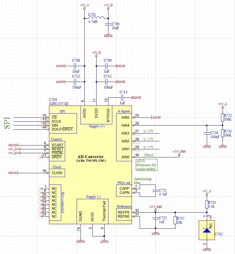
First I try to describe our used configuration of the AD1235. We have an external +2.5V reference on REFP0/REFN0 and also connect this +2.5V to AIN0 as reference input for a single-end measurement.
The input voltage range of our application (single-ended) is 0.35 .. 4.7V and we use the internal PGA with gain=1.
Here the simplified schematics:

Now comes my question:
All measurements where we use the internal VCOM seems to be wrong (e.g. "VCOM-AIN0" or "VCOM-AIN5"). All other measurements get a result as expected.
The internal voltage VCOM is defined as "(AVDD+AVSS)/2", so in our applications it's VCOM = +2.5V.
Is there something special to consider when useing the internal VCOM?
(As example, if we measure "VCOM-AIN0", we expect a converted result of 0V (+2.5V on both PGA inputs => differential 0V), but in real we get a result far away from 0V)

Here are the register settings we used for the measurements:

Best regards
Oliver

  • Here the simplified schematics:

    Here are the register settings we used for the measurements:

  • Hi Oliver,

    Have you measured the +2.5V reference with a DMM as a sanity check to see if it is providing the expected voltage?

    If the external reference is biased with respect to AVSS, as it appears to be in the schematic, then AIN0-VCOM should result in a near zero differential votlage measurement. NOTE: VCOM is internally generated by a resistor divider so it is not a precision voltage reference.

    Regarding the schematic, I don't see where AGND and DGND connect. These should be at the same potential and connected together for the device to work as expected. See https://e2e.ti.com/support/data-converters/f/73/p/755516/2790926 for additional details.

    Also, I would be cautious about using an inductor on the supply pins of any IC, especially a digital device that could have fast transient currents. For one, the inductor might generate large voltage spikes on the supply under transient current and also, because the L+C combination may resonate and result in unexpected circuit behavior.

  • One more quick comment... the register settings for the INPMUX register didn't make much sense to me. To measure AIN4 - AIN0 (for example) you would program INPMUX to 0x51 (or 0x15 to measure AIN0 - AIN4). Check to make sure the input MUX is programmed correctly for each of your configurations.

    CORRECTION: Please disregard my last comment, I was referencing the ADS1261's register values when reviewing you're register settings. For the ADS1235 these values look correct.

  • Hi Chris

    Thank you for your reply and comments. Of course we connect AGND and DGND directly together (at one point), I just forgot to show it in my simplified schematics.
    According to the remark of the used supply inductor, we use that just for filtering of the analog supply voltage. The digital supply voltage is before the inductor. Simplified our supply path looks like follows:

    We still have the same problem, getting wrong measurement results when using the internal Vcom voltage.
    In our application with a +5V to GND Supply the internal Vcom is always (more or less exactly) +2.5V, right?

    We did some tests with internal and external reference voltage, as well as with and without used PGA.
    From Software side we do following sequence (without internal ADC calibration):
         1) setting all registers
         2) starting convertion
         3) reading convertion data
    Here are some measurement results, the yellow marked doesn't make sense for us, the green marked are fine.

    Best regards
    Oliver

  • Hi Oliver,

    I highly recommend removing the inductance between the AVDD and DVDD as Chris mentioned in an earlier post.  What we have seen on various ADCs is the added inductance (even ferrites) will choke required current needed by the ADC in conditions where the internal reference is powered on as well as powering up analog components from a low power or powered down state.  If you need or want some additional filtering I would suggest that you use a small value of resistance instead to create a low-pass RC filter.

    I agree that what you are seeing is unusual and I would actually prefer to see raw codes as opposed to calculated.  You should not see the same voltage for 5V reference as you do for 2.5V.  Have you checked to see if there is some analog settling taking place by taking a series of continuous conversions as opposed to single conversion measurement?

    It is quite possible that VCOM takes some time to establish a constant voltage.  It is also quite possible that due to choke current on the analog supply some odd anomaly is taking place internal to the device.

    Best regards,

    Bob B