Hi,
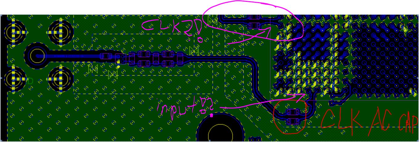
I am trying to design with ADC12DL3200 in single Channel mode at 6GSPS, 4-Bus, Staggered-Mode Timing (LDEMUX = 1, DES_EN = 1, LALIGNED = 0) as datasheet figure 6. the ADC use external input device clock 3GHz and steady before ADC power on.
now i can access all registers via SPI correctly, I followed the initialization set up on datasheet 8.3 part to initialize ADC.
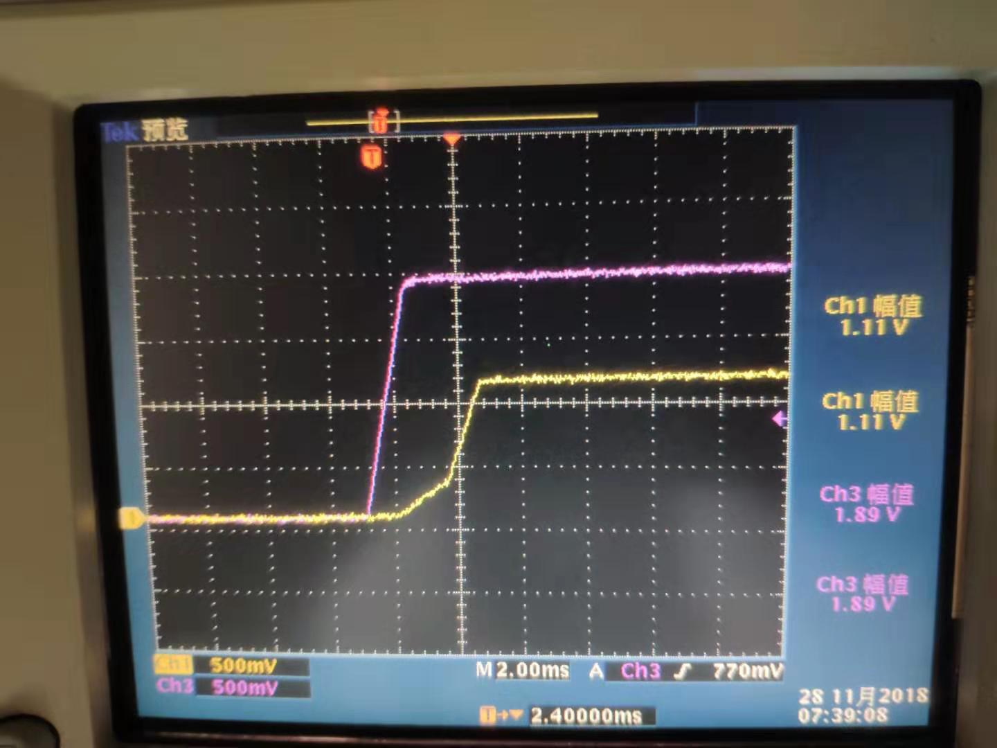
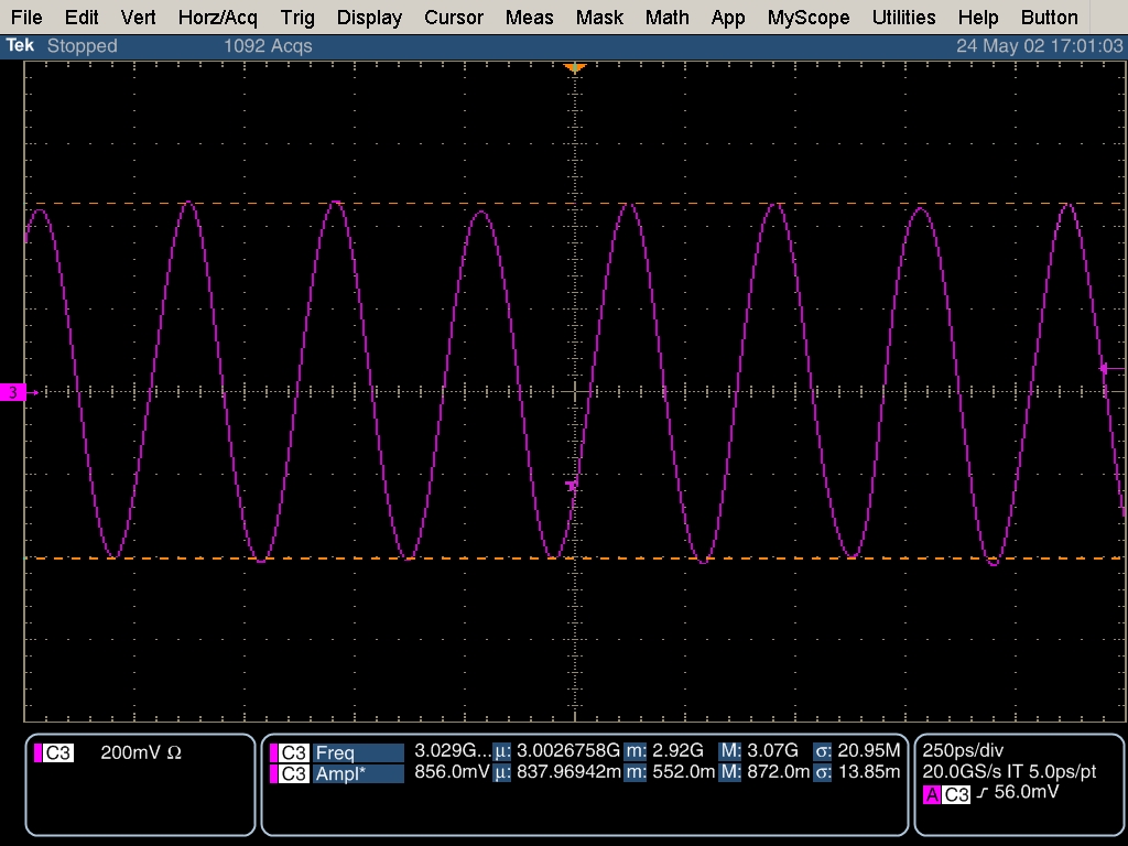
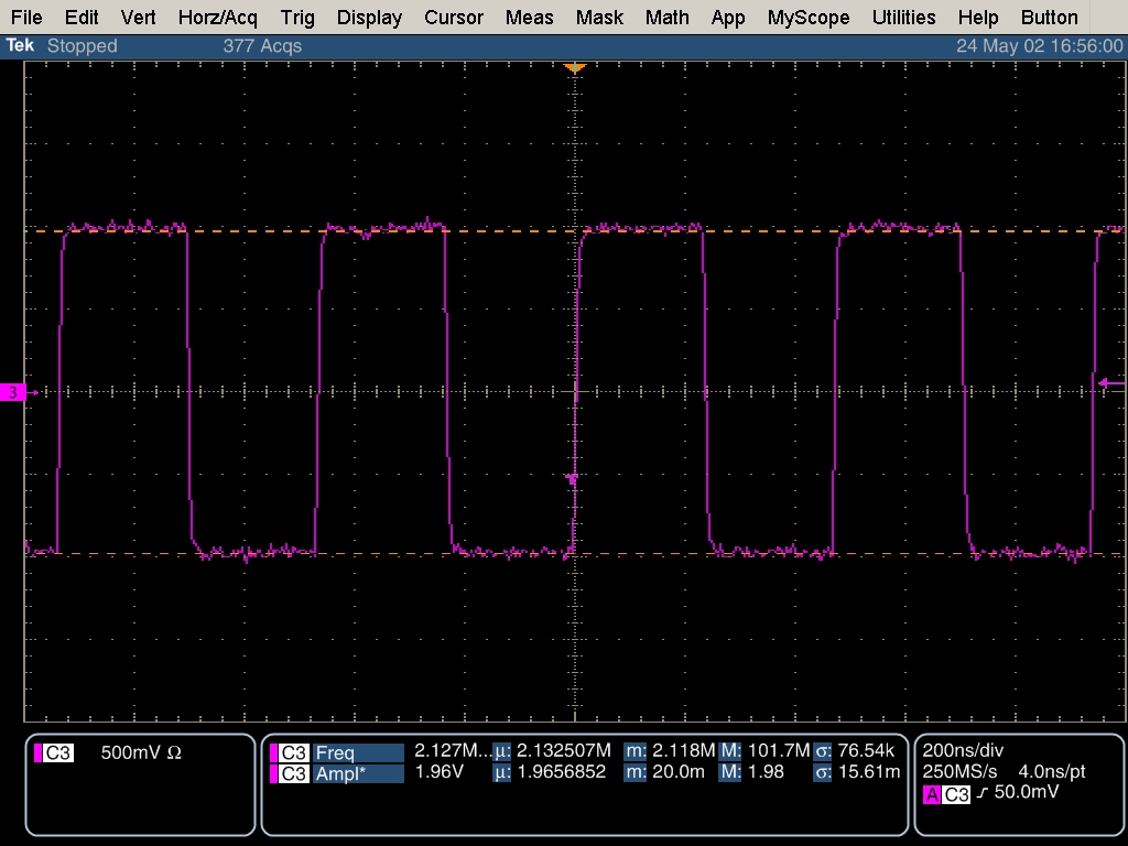
but on FPGA side, i failed to get lock to the DxCLK, i tested the DxCLK with high speed oscilloscope on my board, which surprised me that frequency of all the 4 LVDS buses DxCLKs are ~2.12M instead of 750MHz as I supposed. the 2.12MHz clock is stable with very good SI. and this clock show up once power on even no 3GHz device clock enabled or FPGA firmware download.(equal to disconnect all the SPI/LVDS to FPGA) .
NO sysref/TMSTP provided since only single ADC used on my project.
Do you think the DxCLK behave correctly? why is 2.12MHz ? if it's not correct behavior, any suggestions to further debug on this situation?
Thanks a lot.