This thread has been locked.

If you have a related question, please click the "Ask a related question" button in the top right corner. The newly created question will be automatically linked to this question.

ADS54J66EVM: Wrong ADC sample data. Not receiving sine wave

Part Number: ADS54J66EVM

Setup - Xilinx ZCU102 directly connected to ADS54J66EVM on HPC1.

JESD parameters -

Subclass 1, LMFS = 4421, K = 32, RefClk =  153.6MHz, RxCoreClk = 76.8MHz, Line Rate = 3.072 Gbps, Sysref = 3.2MHz

ADS54J66 parameters -

Sample Clk = 153.6MHz, DDC mode = 8 (direct sampling)

Fin = 644MHz at 10dbm

ADC config sequence

ADS54Jxx_ANALOG
0x00 0x81
0x8020 0x00
0x8021 0x00
0x8022 0x00
0x8026 0x00
0x8053 0x80
0x8055 0x00
ADS54Jxx_DIGITAL
0x6800f7 0x01 //digital top reset self clearing
0x680000 0x01 //reset digital page 6800h
0x680000 0x00 //clear digital page reset
0x690000 0x80 //CTRL K
0x690001 0x01 //JESD mode 20x
0x690002 0x00
0x690003 0x00
0x690005 0x00
0x690006 0x1F //K 32
0x690007 0x08 //subclass 1
0x690016 0x00
0x6A0016 0x02 //PLL mode 40x
0x614100 0x08 //mode 8
0x614101 0x00
ADS54Jxx_LOWLEVEL
0x4003 0x00
0x4004 0x00

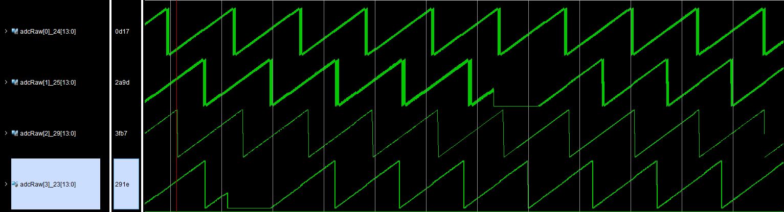
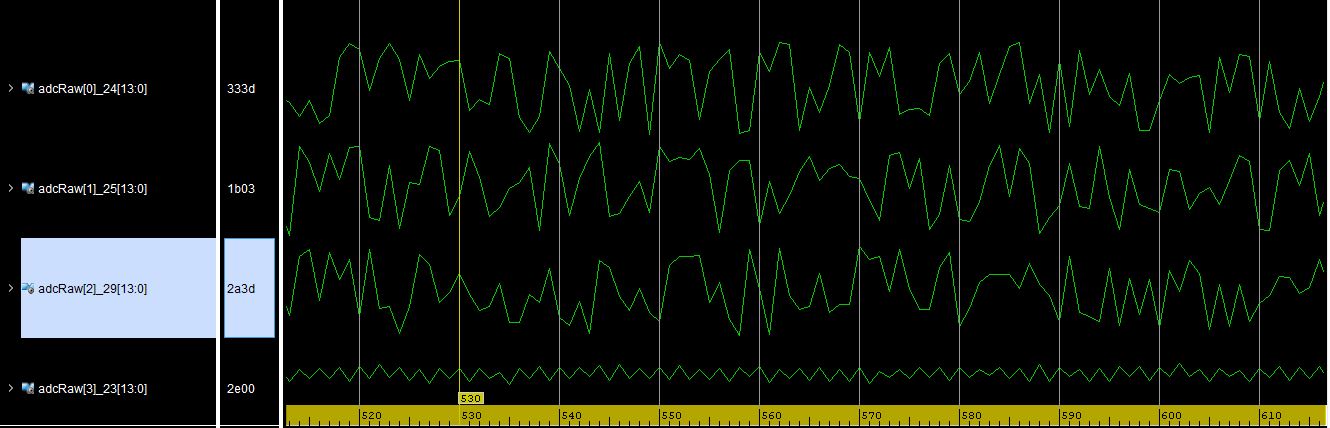
The ADC raw sample data does not look like a sine wave. I have connected output from a signal generator to ADC inputs A, B and C though a splitter whereas input D is left disconnected.

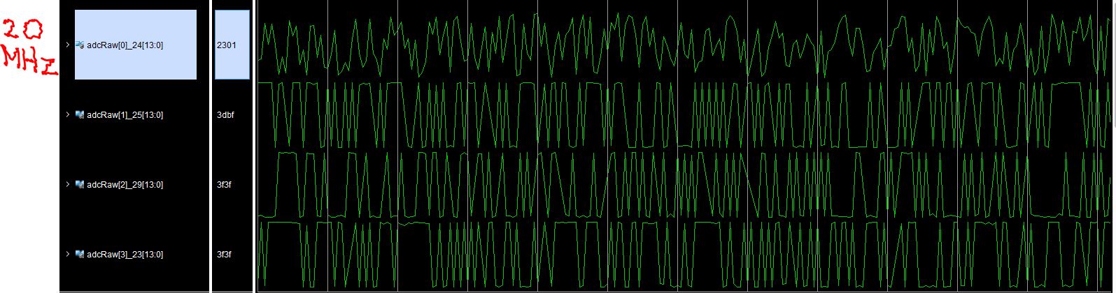
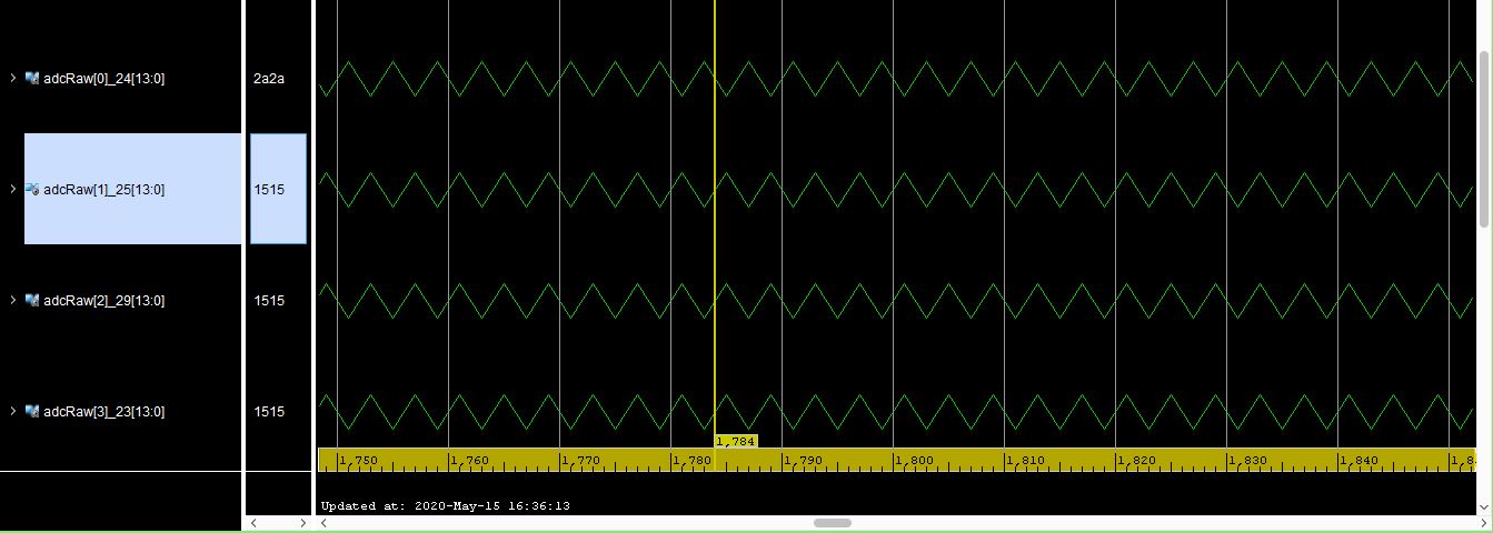
I tried the built-in test patterns in the ADC and was able to see correct ADC sample data for ramp pattern and toggle pattern. While in testmode I disabled interleaving engine 0x680018 (write 0x03) and DC correction 0x0x680068 (write 0x06).

I can also see the ADC lanes are not synchronous, there is a slight phase offset between them. Is the configuration sequence and the setup I am using correct ? 

  • Rajk,

    Your SYSREF value appears to be incorrect. Max SYSREF = Fs/(K *N)  where N is a whole integer. Your max SYSREF should be 153.6MHz / 32 = 4.8MHz. You cannot get to 3.2MHz with N = integer. Try using 2.4MHz. 

    Also, since you are under sampling, I am not sure your waveform is going to show the cleanest sine wave. Try using a lower IF just to verify the part is working properly. Attached is the config file I used to test this setup. 

    Regards,

    Jim 

    8867.ADS54J66_bypass_4421_K32.cfg

  • Thank you, Jim for your quick response. I appreciate your time and help. I set SYSREF to 2.4MHz by changing the sysref divider value to 1024 (VCO 0 frequency is 2457.6MHz). I tried the ramp pattern and observed occasional erratic behavior. The ramp drops midway while ramping and stays low for a few cycles before ramping again. 

  • I would also like to confirm the ADC sample data demapping with you. I am demapping 32bit JESD data frame as below -  

    lane0_tailbits1  <= rxdata[1:0];                                 //0,1 are tail bits                                        
         
    lane0_sample1  <= {rxdata[15:8],    rxdata[7:2]};                  
         
    lane0_tailbits0  <= rxdata[17:16];                            //16, 17 are tail bits
         
    lane0_sample0 <= {rxdata[31:24], rxdata[23:18]};

  • Rajk,

    The ADC sampling map is correct.

    See the ramp pattern file attached.  This is data from our TSW14J56EVM, which is a capture/pattern generator board that TI sells to support this ADC EVM. You will notice this test pattern does not generate the perfect ramp. There is a small dead spot at the end of each complete cycle. 

    Regards,

    Jim

    2783.ADS54J66_ramp_test_Mode_8.pptx

  • Hi Jim,

    Thank you for your help. As per your suggestion, I lowered the input frequency to 20MHz at 5dbm but did not observe a sine wave on the FPGA. I connected the signal generator to input A and left B, C and D disconnected. I also probed the output of the transformer between SMA connector and ADC on the evaluation board and could see 20MHz sine wave there. I used the configuration file you attached in your reply above.

  • Rajk,

    After power and clocks are provided to the ADC, press the reset button on the board before loading the ADC registers. Try lowering the frequency of the input  even more and use the ILA tool to look at the individual bits. This may provide clues to see how the data ordering is being processed. 

    Regards,

    Jim

  • Hi Jim,

    I followed your suggestion and lowered the input frequency to 1MHz on input A of the ADC. I left inputs B, C and D disconnected. I observed the data coming out on the AXI stream bus of JESD receiver module. I noticed, if I swap the upper and lower byte of lower 16 bits [15:0], the control bits or tails bits are present at bit 7 and bit 6. I assumed bits 7 and 6 are tail bits because they are always 0.

    If I remove bits 7 and 6, I see a cleaner sine wave.

    When I observed the upper 16 bits [31:16], I noticed bit 20 is always zero. I assumed bit 20 and 21 to be tail bits and removed them.


    After removing bits 20 and 21 and swapping the bits (based on my observation of [15:0]) as shown in the attached photo, I see a cleaner sine wave.


    However, the upper 16 bits [31:16] sample is not as clean as the lower 16bits [15:0] sample. I believe it may be because bits [31:28] have same value.


    This frame mapping looks significantly different than the ADC datasheet and PG066 AXI stream data mapping. I have also noticed a pattern on the 128bit AXI stream data bus, where bits 6, 20, 34, 48, 62, 76,90, 104, 118 are 0 (every 14th bit is 0 starting from bit 6). I assumed these are control bits along with the next adjacent bit. eg - bit 6 and 7, bit 20 and 21 and so on.  

  • 8585.ZC706 ADS54J66 4421 Setup.pptxRajk,

    We have tested this EVM in the 4421 mode using a ZC706 with our TSW14J10EVM. The source code for this project can be downloaded from the TSW14J10EVM product folder on the TI website. See if this helps with your issue.

    Regards,

    Jim

  • Thank you Jim for your continued help. After investigating further, I found the GT data coming out of the JESD PHY module has the control bits in the correct position but somehow it was getting incorrectly mapped on the AXI Stream data bus.

      
    The tail bits in the lower 16 bits [15:0] are 8 and 9. I swapped the upper and lower bytes and removed bits 8 and 9 to get a clean sine wave. Is it correct tails bits are bits 8 and 9 for [15:0]sample and bits 24 and 25 for  [31:16] sample? 

  • I was able to get correct sine wave by changing AXI stream data mapping to -

          
          lane0_control0   <=  rx_tdata[9:8];                                                                                        
          lane0_sample0  <=  {rx_tdata[7:0],     rx_tdata[15:10]};                  
          lane0_control1   <=  rx_tdata[25:24];                                           
          lane0_sample1  <=  {rx_tdata[23:16], rx_tdata[31:26]};

    The problem with incorrect data mapping was also because of Vivado synthesis flow. I had to make changes in the flow along with the mapping change to get correct data. 

    I appreciate your time and help. Thank you