This thread has been locked.

If you have a related question, please click the "Ask a related question" button in the top right corner. The newly created question will be automatically linked to this question.

DAC37J82EVM: DAC configuration for setting up loopback with ADS54J66.

Part Number: DAC37J82EVM
Other Parts Discussed in Thread: ADS54J66EVM, , ADS54J66, DAC37J82, LMK04828, DAC5675A, DAC38J82

Setup - ZCU102 connected to ADS54J66EVM on HPC1 and DAC37J82EVM on HPC0.

ADS54J66 parameters - LMFS = 4421, K = 32, 307.2MSPS, Line rate = 6.144Gbps, Sysref = 2.4MHz, Mode 8 (bypass DDC), VCO 0 = 2457.6MHz

Input Frequency - 70MHz on all 4 ADC channels

FPGA RX JESD  -  4 lanes, Refclk = 153.6MHz, Coreclk = 153.6MHz, CPLL, LIne rate = 6.144Gbps

FPGA TX JESD - 8 lanes, Refclk = 153.6MHz, Coreclk = 153.6 MHz, CPLL, Line rate = 6.144Gbps

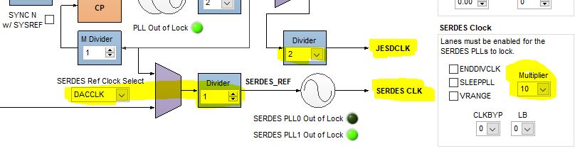
DAC37J82 parameters - ?

I'm looking to set up a loopback where the incoming real sample data from 4 channels of ADS54J66 is sent to either 1, 2 or all 4 channels of DAC37J82. The real sample data sent to DAC does not necessarily have to be for all 4 channels. It can only be for 1 channel (either A, B, C or D).  eg - ADC channel A to DAC channel A. 

I'm setting this up to test the JESD interface between FPGA, ADC and DAC and get familiar with the data converters. 


I'm using a 128 in, 256 out FIFO in between JESD RX and TX module. I have set up the FPGA JESD TX module for 8 lanes only because DAC37J82 has 8 lanes, but if less lanes are used (LMF 222 or 421), the remaining bits on the 256bit AXI Stream bus are set to zero. 

Could you please confirm this setup and suggest a configuration for DAC37J82. Do I have to synchronize the LMK04828 chips on the DAC and ADC EVM with an external reference clock ? Thank you  

  • Hi,

    It is best to use the same LMFS mode per channel and also same SerDes rate. Please see below for example (more info please refer to datasheet/user's guide)

    RajK said:
    Could you please confirm this setup and suggest a configuration for DAC37J82. Do I have to synchronize the LMK04828 chips on the DAC and ADC EVM with an external reference clock ?

    It is best to synchronize the two LMK04828 devices on the EVMs to the same 10MHz reference. The on-board setup of the DAC37J82 supports the dual PLL locking onto the 10MHz external reference.

    -Kang

  • LMK_DAC_2221_307p2MSPS.cfg


    Thank you for your help, Kang. I followed this sequence - 

    Establish ADC link

    1) Program FPGA and reset FPGA JESD RX
    2) Program LMK and wait for PLL1 and PLL2 LOCK (10MHz reference clock 5dbm)
    3) Program ADS54J66
    4) Remove FPGA JESD reset and trigger sysref 
    5) rx_sync goes high and FPGA starts receiving ADC sample data

    Establish DAC link

    1) Reset and clear FPGA JESD TX
    2) Program LMK and wait for PLL1 and PLL2 LOCK (10MHz reference clock 5dbm)
    2) Observe K28.5 characters (0xBCBC) on GT lanes
    3) Toggle DAC RESETB pin button in the Quick Start page of DAC3xJ8x GUI
    4) Program DAC and read alarms
    5) RESET DAC JESD and trigger sysref
    6) Read alarms

    After this sequence, tx_sync goes high and I can see real sample data on the GT lanes but I see a FIFO Empty Error and no analog output on any channel.


    I have attached the configuration files for LMK and DAC here. 

    DAC_2221_may27.cfg

  • Hi,

    this is probably due to the ADC only send out 2 lanes of data, while the DAC is expecting 8 lanes of BCBC code. You can mitigate this by setting the 2 lanes on the DAC to link 0, while the other lanes to link 1. To do so, do the following:

  • DAC_2221_may27_updated.cfg

    HI Kang,

    Thank you for the suggestion. I made these changes but tx_sync does not go high. The clock to DAC is 307.2MHz and the serdes PLL output is 10x (3072MHz), whereas the JESD clk is 153.6MHz . I've set the rate to Eighth. Is this configuration correct ? Sysref is 2.4MHz. I have attached the configuration file here.


  • Hi 

    The main menu configuration tool should set these automatically. Could you please rerun the automation configuration tool to double check?

  • Hi Kang,

    I am following this sequence 

    1) Reset and clear FPGA JESD TX
    2) Program LMK and wait for PLL1 and PLL2 LOCK (10MHz reference clock 5dbm)
    2) Observe K28.5 characters (0xBCBC) on GT lanes
    3) Toggle DAC RESETB pin button in the Quick Start page of DAC3xJ8x GUI
    4) Program DAC 
    5) RESET DAC JESD and trigger sysref
    6) Read alarms


    The main page looks like this all along the flow. No matter what setting I pick in the "number of serdes lanes" or "interpolation" or "DAC Data rate", the Clocking page settings remain the same . Could you please share a configuration file for the DAC and LMK. Could you please also share steps to bring up the DAC and provide more information on the serdes clk, serdes PLL, JESD clk and Lane rate setting (on the "serdes and lane configuration" page). Thank you 


  • After following the sequence mentioned in the post  https://e2e.ti.com/support/data-converters/f/73/t/582952   I was able to achieve sync and there were no FIFO errors.
    DAC_2221_postsync_may27.cfg

  • I setup the ADC input frequency to 644MHz at 5dbm and observed multiple tones at the analog output of DAC. 


    Interpolation 1 -


    Could you suggest a configuration for both ADS54J66 and DAC37J82 such that the analog output of DAC is single tone at 644MHz. The setup is same as original, sending real ADC sample data to DAC. 

  • Hi,

    This looks like you may need to do additional post processing (filter through FIR implementation and proper scaling) to get good DAC output. The noise floor of the ADC was not filtered digitally, and there are scaling issues as the signal is distorted.

    you can try to enable DAC37J82 constant output with NCO set at 644MHz. This should give you a good idea on whether the DAC is operating correctly or not.

    -Kang

  • hi,

    Steps to do constant output of the DAC

  • I appreciate your time and help, Kang. I tried setting the NCO and observed a weak tone at 644MHz. 

    I am migrating from an LVDS based DAC (DAC5675A) design to JESD DAC (DAC37J82) design. The sequence of the complex data sent to DAC5675A was I_P -> Q_P -> Q_N -> I_N

              I_P <=   {~I [15], I [14:0]};
              I_N <=   {I [15], ~I [14:0]};
              Q_P <= {~Q [15], Q [14:0]};   
              Q_N <= {Q [15], ~Q [14:0]};  

    I would like to know if this IP, QP, IN, QN complex data can be sent to DAC37J82. Can I bypass the mixer inside the DAC in this case and still get an analog output? 

    The IP, QP, IN, QN data is updated in the FPGA at 10MHz and sent to DAC37J82 at 858.66MHz. The desired analog output frequency is 644MHz and DAC sampling frequency is 858.66MHz. Could you please suggest a DAC configuration for this use case ? I currently have JESD link setup as external clock, LMFS 8212, Line rate = 4.2933Gbps, Interpolation 1. 

    Should I create a new post for this question ?

  • Hi,

    To answer your questions:

    RajK said:

    I am migrating from an LVDS based DAC (DAC5675A) design to JESD DAC (DAC37J82) design. The sequence of the complex data sent to DAC5675A was I_P -> Q_P -> Q_N -> I_N

              I_P <=   {~I [15], I [14:0]};
              I_N <=   {I [15], ~I [14:0]};
              Q_P <= {~Q [15], Q [14:0]};   
              Q_N <= {Q [15], ~Q [14:0]};  

    I would like to know if this IP, QP, IN, QN complex data can be sent to DAC37J82. Can I bypass the mixer inside the DAC in this case and still get an analog output? 

    This can be down. Simply enable 2's complement format setting on the DAC37j82

    Yes, you can bypass complex mixer to output directly the baseband data

    RajK said:

    The IP, QP, IN, QN data is updated in the FPGA at 10MHz and sent to DAC37J82 at 858.66MHz. The desired analog output frequency is 644MHz and DAC sampling frequency is 858.66MHz. Could you please suggest a DAC configuration for this use case ? I currently have JESD link setup as external clock, LMFS 8212, Line rate = 4.2933Gbps, Interpolation 1. 

    The DAC is designed to operate for 1st Nyquist zone. To output 644MHz, you will need at least twice the sampling rate. I recommend increase interpolation to increase the sampling rate for 1st Nyquist zone operation.

    -Kang


  • Hi Kang,

    Thank you for your help. The FPGA is sending 4 IQ samples to DAC as mentioned in my previous reply (+I, +Q, -I, -Q). I have tested the DAC in the following two configurations - 

    1)
        Output frequency - 644MHz (3rd harmonic), fundamental = 858.66/4 = 214.66MHz
        Sampling frequency - 858.66MHz
        FPGA core clk - 107.33 MHz
        Line rate - 4.293 Gbps


    2)

       Output frequency - 1.0136GHz (5th harmonic), fundamental = 810.88/4 = 202.72MHz
       Sampling frequency - 810.88MHz
       FPGA core clk - 101.36 MHz
       Line rate - 4.054 Gbps

    For both the above two configurations LMFS = 8212, K = 32, two's complement format and bypass complex mixer. This setup is NOT looping back ADC data to DAC. In this setup the FPGA is generating IQ data.

    The output of DAC contains multiple tones spaced "coreclk" frequency apart. Is this an expected behavior of DAC ? Is it expected to see sub harmonics along with harmonics at the output of DAC?

     1) 644MHz. The spacing between tones is 107.33MHz


    2) 1.0136GHz. The spacing between tones is 101.36MHz


    Is there a way to get rid of the sub harmonics (may be using complex mixer in DAC) ? I'm going to use a bandpass filter at the output of DAC to filter out all the other harmonics and only pass the desired output frequency.  

  • Hi,

    most likely you are driving the digital path too hard and exceeded the full-scale. Please try to back-off the data by reducing the digital code and recheck.

    -Kang

  • Hi Kang,

    Thank you for the suggestion. I realized that the IP, QP, IN, QN samples are actually being sampled by two converters on the DAC. I'm looking to send all the four IP, QP, IN and QN samples to only one converter. I'm looking to send only one sample every DAC sample clock as below -

    DAC sample clock cycle 1 - IP
    DAC sample clock cycle 2 - QP
    DAC sample clock cycle 3 - QN
    DAC sample clock cycle 4 - IN 

    DAC sample clock is 858.66MHz. By sending one sample per DAC sample clock I expect to see fundamental frequency at 858.66/4 =  214.66MHz and its harmonics at 429.33MHZ, 643.98MHz, and so on. 

    Do you have recommendation for the frame assembly on the FPGA side ? Do you recommend using LMFS 8212 or 4211 for this application?

  • Hi Rajat,

    the following is not possible for discrete DAC. Each DAC is meant to take either I or Q. For your setup below, you will need a quad DAC to send the two streams of I/Q signal into four separate DACs.

    RajK said:
    Thank you for the suggestion. I realized that the IP, QP, IN, QN samples are actually being sampled by two converters on the DAC. I'm looking to send all the four IP, QP, IN and QN samples to only one converter. I'm looking to send only one sample every DAC sample clock as below -

    DAC sample clock cycle 1 - IP
    DAC sample clock cycle 2 - QP
    DAC sample clock cycle 3 - QN
    DAC sample clock cycle 4 - IN 

  • Thank you for the info. We are flexible with our design and can make changes to make it work with dual DAC DAC37J82. We are migrating from DAC5675A and in our experience with DAC5675A, the FPGA was sending samples like below such that the fundamental frequency would appear at 1/4th of the DAC sampling frequency that gave us flexibility to pick any harmonic from the DAC analog output. 

    DAC sample clock cycle 1 - IP
    DAC sample clock cycle 2 - QP
    DAC sample clock cycle 3 - QN
    DAC sample clock cycle 4 - IN 


    When we migrate to DAC37J82, we are hoping to recreate the same scenario where the fundamental appears at 1/4th sampling frequency. Our design's desired signal is 644MHz and it can either be the fundamental frequency or a harmonic at the analog output of DAC. So far, I have tried the following configurations -

    1) LMFS 8212, Line rate 4.293Gbps, DAC clock = 858.66MHz, FPGA core clock = 107.33MHz

    Lane 0  IP[15:8] IP[15:8] IP[15:8]
    Lane 1 IP[7:0] IP[7:0] IP[7:0]
    Lane 2 IN[15:8] IN[15:8] IN[15:8]
    Lane 3 IN[7:0] IN[7:0] IN[7:0]
    Lane 4 QP[15:8] QP[15:8] QP[15:8]
    Lane 5 QP[7:0] QP[7:0] QP[7:0]
    Lane 6 QN[15:8] QN[15:8] QN[15:8]
    Lane 7 QN[7:0] QN[7:0] QN[7:0]


    2) LMFS 8212, Line rate 4.293Gbps, DAC clock = 858.66MHz, FPGA core clock = 107.33MHz

    Based on your previous reply where you suggested to not drive the digital path hard, I modified the frame assembly such that every second sample is 0. I interpreted "not drive digital path hard" as reducing the number of samples going from FPGA to DAC.  

    Lane 0 IP[15:8] 0 IP[15:8]
    Lane 1 IP[7:0] 0 IP[7:0]
    Lane 2 IN[15:8] 0 IN[15:8]
    Lane 3 IN[7:0] 0 IN[7:0]
    Lane 4 QP[15:8] 0 QP[15:8]
    Lane 5 QP[7:0] 0 QP[7:0]
    Lane 6 QN[15:8] 0 QN[15:8]
    Lane 7 QN[7:0] 0 QN[7:0]

    The AXI -Stream data bus for 8 lanes is 256bit wide for Xilinx JESD module and according to frame assembly from page 29 of DAC37J82 datasheet, there are 192bits (twelve 16bit samples). Samples written to the AXI-Stream data bus are as below -

    [255:0] tx_tdata;

    tx_tdata = {64'b0, twelve 16bit samples}; 

    The AXI-stream data bus operates at FPGA core clock 107.33MHz. 

    The DAC output for both these configurations was this - 


    Here, all the tones were harmonics of the FPGA core clock 107.33MHz. The desired frequency 644MHz was the 6th harmonic. Could you please recommend a configuration such that the DAC output will have fundamental frequency at 214.66MHz and its harmonics at 429.33, 643.98 and so on. We can modify the number of lanes used, sampling frequency, line rate, frame assembly, etc. 


  • Hi

    RajK said:
    Thank you for the info. We are flexible with our design and can make changes to make it work with dual DAC DAC37J82. We are migrating from DAC5675A and in our experience with DAC5675A, the FPGA was sending samples like below such that the fundamental frequency would appear at 1/4th of the DAC sampling frequency that gave us flexibility to pick any harmonic from the DAC analog output. 

    DAC sample clock cycle 1 - IP
    DAC sample clock cycle 2 - QP
    DAC sample clock cycle 3 - QN
    DAC sample clock cycle 4 - IN 

    You point above has nothing to do with the feature of the DAC5675A or the DAC38J82. It is a simple Fs/4 quadrature mixing without actually utilizing sin/cos arithematics.

    Simply substitute equation found in 7.3.12 section of the datasheet with Fs/4, you can find the sine portion is going to zero, and there are sequence of -/+ I and Q stream to form simple Fs/4 modulation without arithematics. 

    RajK said:
    Based on your previous reply where you suggested to not drive the digital path hard, I modified the frame assembly such that every second sample is 0. I interpreted "not drive digital path hard" as reducing the number of samples going from FPGA to DAC.  

    When I say not driving too hard, I mean you have to be careful with the scaling of the sine/cosine wave to not exceed 2^15 signed binary. It has nothing to do with the length of the waveform. 

    -Kang

  • Thank you for the suggestion, Kang. It helped me make progress with my design. I changed the JESD configuration to LMFS 4211, FPGA core clk = 202.72MHz, Line rate = 8.1088Gbps and DAC sample freq = 810.88MHz. Here the desired frequency is 1013.6MHz (5th harmonic of 202.72MHz) and the output of  DAC has tones at 202.72MHz, 405.44MHz, 608.16MHz, 1013.6MHz and so on. This is an expected DAC output, however the signal is too weak. 

    The IQ sample data being sent from FPGA to DAC is in twos complement format. Below is DAC output - 


    The Coarse DAC gain is set to 15. (write 0xF300 to register config3 0x03 ). Do you have recommendation on how to get stronger output ? Is it related to the data format (twos complement or offset binary) ?

    The 16bit +/- IQ data is 7FFF, 8000 in twos complement format.

  • Hi,

    The DAC current is already at the maximum. This is the DAC output stage. The datasheet describes the DAC output stage operation and how the input data code is related to it.

    To get stronger DAC output, you will need external amplifier.

    -Kang

  • Hi Kang, 

    Thank you for your help. I had the lane IDs in the "Serdes and Lane configuration" page of the GUI set as 0, 1, 2, 3. After changing these lane IDs to 3, 2, 1, 0 the DAC output looks much better. I am now seeing errors on Lane 4  (Multiframe Alignment error, Frame alignment error, CGS error and Not in table error). There is a FIFO write full and FIFO read error on this lane too. (see photo below)

    I have configured the serdes lanes as per your previous guideline. The active lanes are on Link 0 and the unused are on link 1. 


    Is it safe to ignore these errors on Lane 4 ? 

  • Hi Raj,

    If you are not using the lane 4 (based on your description), then you do not need to pay attention to lane 4 errors. Thanks for the update.

    -Kang

  • Thank you for the recommendation. I am designing a custom board with DAC37J82 and I am following the DAC37J82EVM board schematic as reference. I am looking for guidelines on separating DGND and AGND pins in the schematic. I am also looking for guidelines on isolating AGND and DGND planes in layout. Do you have recommendations on that ?

  • That link is helpful. Can you provide .brd file of the DAC EVM board. I downloaded the board files from TI website but it does not contain the .brd file. 

  • brd file attached

    DAC3XJ8X_D.brd

  • Thank you for the file, Kang. Are there in-pad vias under the DAC chip ?

  • yes, confirmed

  • Hi Kang,

    Thank you for confirming that. We would like to request phase noise data of the DAC37J82 chip for frequency offset between 1Hz - 100Hz. Is it possible for you to provide it ? I came across this post https://e2e.ti.com/support/data-converters/f/73/t/648676  where the phase noise data provided was for frequency offset > 1kHz. Thank you

  • Hi Raj,

    Given the current COVID situation, lab access is scarce. I will need business justification and the scope of work in this. Please contact me offline so I can determine the priority.

    -Kang

  • Sure not a problem, Kang.

  • connecting offline

  • Hi Kang,

    Could you please provide a software to run eye scan on the DAC. Thank you

  • Hi Kang,

    We have designed schematic for DAC37J82 output. Is it possible for you to review it and provide constructive feedback on it ? Thank you

    DAC37J82EVM had a 75 Ohm transformer but our application requires a 50 Ohm transformer TC1-1T-152X+ that has a center tap. 

  • Hi Kang,

    The document mentions I have to request the scan GUI on E2E forum.

  • I also responded to you offline in private message. Could you also please comment on the schematic above. Thank you

  • Is there a question here?

  • Do I have to create a new post for requesting eye scan gui ?

  • No. It can be downloaded from the link below.

    Regards,

    Jim

    txn.box.com/.../ifvfhxkhdrrz4nnwp2clqmd3ayb9nnvz