This thread has been locked.

If you have a related question, please click the "Ask a related question" button in the top right corner. The newly created question will be automatically linked to this question.

ADS122C04: How to drive with INA317

Part Number: ADS122C04
Other Parts Discussed in Thread: INA317, , OPA314

I have watched videos and read articles about how to drive SAR A/D converters but there is only minimal information regarding Sigma-Delta converters.

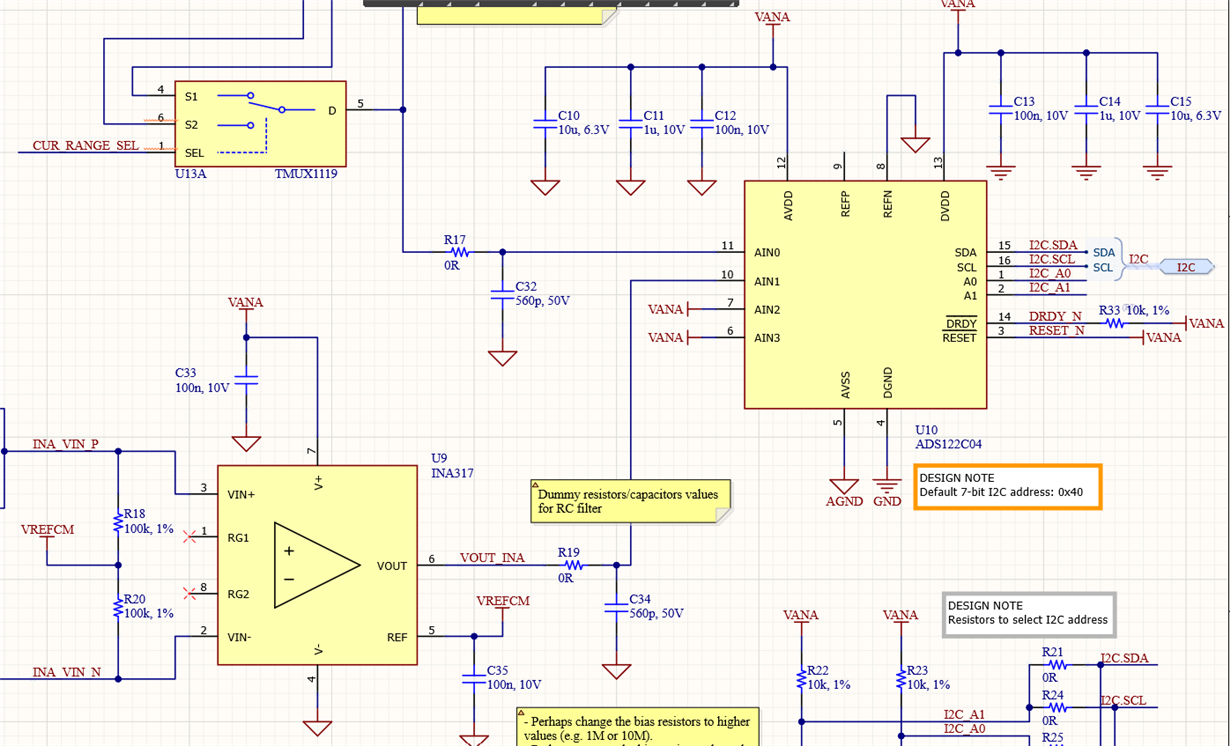
In my application I want to drive an ADS122C04 converter with an INA317. What recommendations should I user for this case?

  • Hi Nikos,

    Do you need to use the INA?  The ADS122C04 has a built in PGA with a gain up to 128.  As far as the drive, the ADS122C04 input is buffered in PGA bypass mode and when using the PGA becomes high impedance, so there are really no input restrictions with respect to driving the ADC.

    However, you would want to have an antialiasing filter at the analog inputs.

    Best regards,

    Bob B

  • Hi Bob,

    thank you for taking the time to answer my question.

    Your suggestion is interesting, because I have considered it myself! It is just that I cannot simulate the PGA of the ADS122C04 and I felt more confident with using an external INA. But without it, things would be much easier.

    I am only using the INA with a gain of 1, so that is not an issue. I have attached my schematic for this part of the circuit. Let me briefly explain.

    My input is a floating differential voltage that can go anywhere withing around +/- 2.2V. For this reason I have chosen VANA to be 5.2V and REFP of the ADC will be connected to 5.0V. VREFCM is VREFP/2 = 2.5V. This is another reason I selected an external INA, because I don't know if I can bias the input voltage at half the ADC range. The anti-aliasing filter at the INA output is not yet correctly dimensioned. Moreover, I have put R18 and R20 to correctly bias the floating input voltage to the INA's input common range, but I was planning to increase their value to be around 10Meg.

    Do you think it would work if I omitted the INA? Can I use again the same 10Meg bias resistors to VREFCM as before? Would these resistors be enough to set the common mode of the input signal to the middle of REFP-REFN, so that I can use almost the full scale of the ADC?

  • Hi Nikos,

    It is difficult to answer with certainty as I do not know anything about the driving source.  Using a similar type method to set the common-mode for thermocouples works well.  The PGA stage for the ADS122C04 is similar to the OPA314 in an instrumentation amplifier configuration.

    I would suggest that you make the two unused inputs of the ADS122C04 to also have a connection, or possibly test points so that you could try both the external INA and the PGA directly of the ADC as a comparison.

    Best regards,

    Bob B

  • Hi Bob,

    thanks again. I have one last question, related to my initial post.
    What is your advice regarding the anti-aliasing filter? In the datasheet it is mentioned it should have a cutoff around the sampling rate or 10x higher, limiting at the same time the R below or equal to 1k. And that f_cutoff should also (obviously) be much lower than the f_mod.

    In my case, I will operate the ADC in a single conversion mode, so my sampling rate will be much lower than 20SPS (lower limit of the ADC in continuous mode). For the sake of simplicity, let's pick this 20SPS. That means the filter has to be at around 200Hz, as per recommendation. With 1k, that means a C of around 800nF. 

    Usually, in a SAR filter I would limit C below 10nF to minimize noise.

    What do you think?

  • Hi Nikos,

    If the input were differential you would have twice the resistance in the filter, so that makes the computation a little easier to target 200Hz fc.  As a general rule I like to keep my resistance values at 4.7k Ohms or less and the capacitor value at 100nF or less.

    What you need to consider is where the noise signal is in relation to fmod/2 (128kHz normal mode).  Let's say you have a noise source at 1kHz that is 65dB below your signal of interest.  You will have a combination of the input filter and the digital filter for your total response. Let's say you design the filter for a cutoff frequency of 340Hz using 4.7k and 100nF.  This combination will already be reducing the 1kHz frequency even further say by about 10-15dB (just a guess I didn't plot) and lets add the low-pass response of the digital filter at 20sps which is probably around another 20-30dB reduction.  With the first order filter response at 20dB per decade you can see that by the time you get to fmod/2 the response of the noise will be very low compared to the signal of interest.  As the filter response continues to fmod, what can alias is in the level of noise of the ADC.

    It the noise voltage is very high, then you would need to come up with a better filter method perhaps using a higher order filter.  However, in most cases you do not require an aggressive input filter when using a Delta-Sigma ADC.

    Best regards,

    Bob B