This thread has been locked.

If you have a related question, please click the "Ask a related question" button in the top right corner. The newly created question will be automatically linked to this question.

ADS7828: Device latched up in error state

Part Number: ADS7828
Other Parts Discussed in Thread: OPA320, INA331

I have an instance where an ADS7828 device appears stuck in a state where it is giving an erroneous digital output for the analog input.

Here are the details:

  • CH3 of device is connected to output of a pressure transducer.

  • Measured DC voltage for CH3: 0.24V.

  • CH3 is selected by this I2C write command: 0xD4

    • Single-ended inputs

    • C2:C0 = 101

    • PD1PD0 = 01 – Internal reference off and A/D converter ON

  • Resulting read value = 0x05AD (1453)


One reason this is suspicious is that this board connects the output of another identical pressure transducer to a 4 channel ADC:

  • Measured DC input voltage: 0.25V

  • Resulting digital output = 0xCD (205)


Given the state of the system when the conversion is done, this result from the 4-channel ADC is what we expect, and we are trying to understand the discrepancy between the ADS7828 result and the 4-channel ADC result.


I can provide data from the other channels of the ADS7828 if needed.

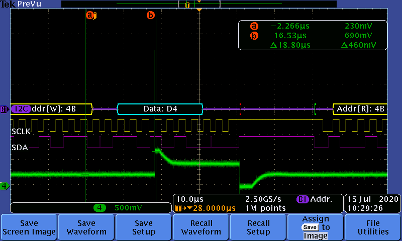
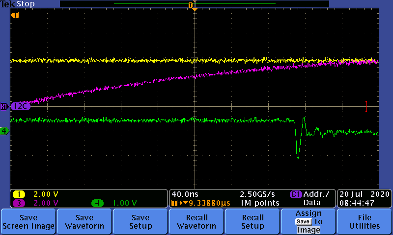
  • Here's an update -- the attached scope picture shows a channel input glitch (the green waveform) right when the ADC starts sampling that channel.

  • Mark,

    I am reviewing your post and will get back with you soon.

  • Mark,

    Before we get started I have a few basic questions/comments:

    1.  Based on your scope waveform, I think you are running in High-Speed (HS) mode.  Did you review the data sheet section "Reading in HS Mode".  In order to read in HS mode you need to write to the device to transition it from F/S to HS mode.  Also, when in HS mode the device does not have enough time to fully complete a conversion.  The ADC should do clock stretching to account for this.  I recommend, simply using F/S mode to avoid this (at least for an experiment).  

    2.  According to your post, you are using an external voltage reference.  What is the value?

    3.  I noticed in your picture that you show a relatively large glitch on the ADC channel input.   What circuit is connected to the input?  To get a valid conversion, we need to fully charge up the internal sample and hold capacitor.  I need to know what the RC filter and signal are to know how long it should take to charge the internal sample and hold.

    4.  I checked your command byte.  This looks correct for single ended, Ch 3, internal ref off, ADC on.  I can also see that the ADC is acknowledging communications.  

    I look forward to your comments on the above points.

  • Art,

    Thanks so much for your reply.

    1. What in the scope waveform indicates High Speed mode? Our SCL frequency = 300 kHz, so that is Fast Mode, isn't it?

    2. The external reference is 4.95V.

    3. Yes, the input glitch and how to get rid of it is the focus of our investigation. The input for ADC channel 3 is being driven by the analog output of an HCE series pressure sensor from First Sensor.

    I have attached the sensor data sheet below.

    ***************************************************************************************

    Some further developments since I wrote the above

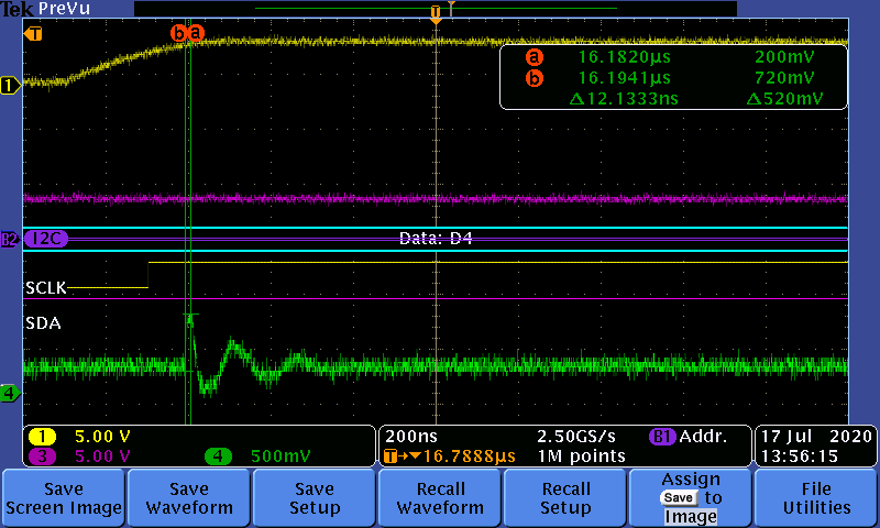
    We attempted to take the ADS7828 device off the board where the large glitch occurred so we could we attach it to a board in our benchtop setup for further study. Unfortunately, we damaged that chip and can no longer use it. We put a new ADS7828 device on the original board. The large (~20us) glitch seen before is gone, and all we see on the scope trace of the channel 3 input at the point where channel 3 starts the conversion process is the small noise seen in the new scope photo below.

    Does the large noise glitch seen previously indicate that the channel 3 circuitry on the old part had been  damaged? If so, can you make any educated guess on the cause of that damage? Is the fact that this board was designed with no RC filter on the channel 3 input a contributing factor?

    HCE series pressure sensors.pdf

  • We have a second unit with the same failure. The first scope trace below show the glitch on the channel 3 input, and the other two have an expanded time base to show the details on the front and back ends of the glitch. I'd appreciate any information or insight you can provide.

    Mark

  • Mark,

    1.  Do you see the glitch if the ADC is not connected?  When the ADC switches from conversion mode to sample mode a 25pF sample-and-hold capacitor is connected to the input of the ADC.  This can potentially create a small transient when the capacitor charges.  However, 25pF is a small capacitance so I wouldn't expect the transient to be very large.  Your scope waveforms show a very large transient and I don't think that would be caused by connecting the sample and hold capacitor.  If this transient is created by some external issue the transient could potentially damage the ADC or put it in a abnormal state.

    2.  I notice on the second waveform that the transient actually goes below GND.  This definitely would not be expected from the ADC sample-and-hold capacitor.  If you disconnect the ADC can you see the same transient?

    3.  Do you have an RC filter between the sensor and ADC?  Can you share a schematic of your ADC connection to the sensor and voltage reference?  Placing a small RC circuit between your sensor and ADC is common practice (e.g. 100 ohms and 1nF).

    4.  Does the transient happen each conversion cycle?  Does the circuit operate correctly until the transient occurs?

  • Art,

    Thanks for your reply.

    1. No, we do not see the glitch if ADC pin 4 (the channel 3 input) is disconnected from the net driven by the sensor. And the glitch returns when we reconnect ADC pin 4 to the net.

    2. That transient is gone when ADC pin 4 is not connected to the net.

    3. No, this board design does not include an RC filter between the sensor and ADC. This board design also does not have a power or ground plane.

    4. As far as I can see, the transient happens during each conversion cycle. In this case, it appears that the ADC always gives a digital output for channel 3 that reflects the glitch, not the expected ~200 mV expected input.

    Do 1 and 2 prove that the ADC is the source of the glitch -- perhaps in concert with the deficiencies of our board design?

    Mark

  • Mark,

    It isn’t unusual to see some kind of transient when the acquisition period starts, as the ADC input connects in a sampling capacitor and the capacitor needs to charge.   However the glitch you see seems rather large. Perhaps you are correct and the lack of a GND plain may play a part here. I looked through the data sheet of your sensor and it doesn’t have much information about the analog output. My guess is that there is some kind of amplifier inside of the sensor but I wonder what the characteristics of that amplifier are. If may be that the amplifier is a low bandwidth and / or high output impedance amplifier and cannot respond to the transient capacitive load from the ADC.

    As an experiment, can you connect an amplifier between the sensor and ADC? The OPA320 is a good choice for driving SAR ADC. You could use a prototype PCB like the DIP-ADAPTOR-EVM to do this test. This kind of amplifier is generally needed in SAR ADC with a faster sampling rate than the ADS7828, but I think this is worth doing as an experiment. Alternatively, if you can disconnect the sensor, and connect a power supply to the ADC input you should get reasonable results. Most power supplies will have low impedance output, and your sensor may not have a low impedance output.

    With regards to you layout / design, it is important to make sure that you have good decoupling that is tightly connected to supply and GND. I understand that you don’t have a GND plane, but I hope you at least have good tight decoupling. Although we recommend a solid GND plane, I would expect that you may get reasonable results for a 12 bit device if you have good decoupling.

    I’m looking back through the question. You mention that you have another 4-channel ADC connected to the same model pressure transducer. What model ADC is giving you the good results? Based on your earlier comments the results are substantially off.  Do you get a consistent error?

  • Art,

    Thanks for your reply.

    Regarding the decoupling, our board design does include 10uF and 0.1uF decoupling capacitors between 5V and digital ground close to each of the ADS7828's.

    The 4-channel ADC that services the mate sensor is an AD7991.On the 2 units I've looked at with this failure, we do see a consistent error. The sensor/ADC pairs are expected to give matching results, but the ADC7991 channel gives a result of ~200 counts, and ADS7828 channel 3 (when the big glitch is present) gives a result of ~1500 counts.

    Since we only see the glitch on some boards, and the glitch disappeared on the board where we replaced the ADS7828 with a brand new chip, I'd like to get your insight on the possibility that the glitch is a symptom of damage on the ADS7828. Our experience has been that we can replace an ADS7828, have it work in a unit for several months, and then see a failure like the one we've have traced back to glitch. As you say, the size of this transient is unusual. So can it be that the parts that exhibit the transient are damaged? And if so, is there any way to tell how they were damaged, and how to prevent that damage?

    Mark

  • Mark,

    Your latest comments really help to clarify the issue. Thanks. I think the glitch does make sense if the device is damaged.

    There are a few ways you can damage a device:

    1. ESD mishandling during or after assembly. Typically you wouldn’t expect ESD mishandling to lead to repeated failures of one particular device in on a board. Since you have seen this on two devices I doubt this is the issue.
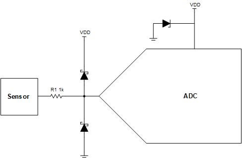
    2. Electrical overstress on input of device. This means that the absolute maximum input signal is violated. One way that this can happen is if the sensor is powered up before the ADC. Another way is if the output of the sensor has a transient voltage above or below the supply of the ADC. In you glitch waveforms I noticed that the input signal seems to go below GND. One simple way to avoid this is to put a current limiting resistor between the ADC and sensor. A better way to avoid this is to also include a Schottkey diode in conjunction with the resistor on the input to shunt overstress signals to GND or supply.
    3. Another way the device can get damaged is with a power supply transient. In some cases a transient on the input can feed through the device to the supply, so it is always recommended to protect the supply. The best way to protect the supply is to include a TVS diode on the supply. The rating of the standoff voltage is equal to the nominal supply voltage and the breakdown should be lower than the Absolute Max supply rating. I think TVS diodes should always be included on supplies for any released product. The cost and size is minimal and the benefit is significant.
    4. Below is a recommended circuit.

  • Art,

    Thanks for your reply.

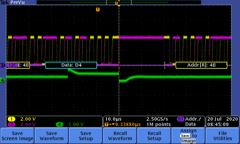
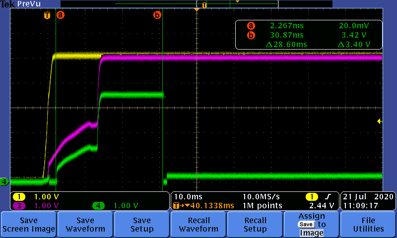
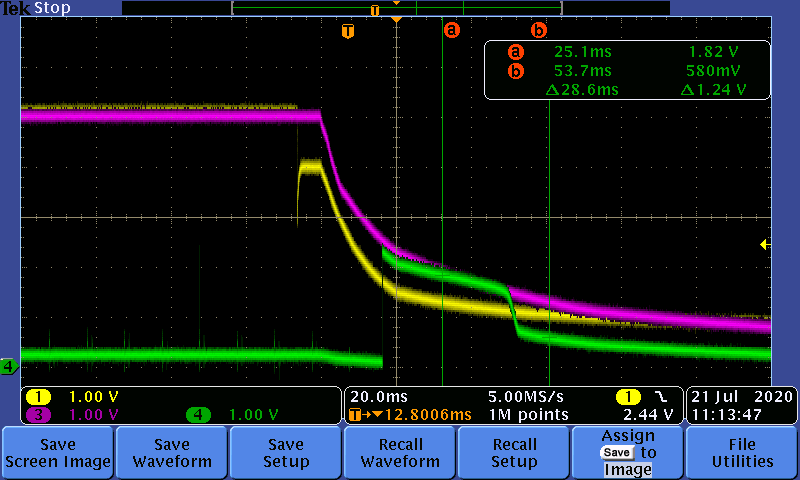
    Regarding the power up sequence of the sensor vs. the ADC, I think that is OK because the sensor is powered by 5Vref, which comes up after the 5V that powers the ADC. The scope trace is below -- yellow = 5V (ADC supply) , purple = 5Vref (sensor supply) and green = sensor voltage output.

    But could what happens at power down damage the device? The scope trace below shows that -- the ADC supply voltage (yellow) falls below 5Vref (purple), and the sensor output has a ~30 ms transient where it is ramping down at a voltage above the ADC supply voltage.

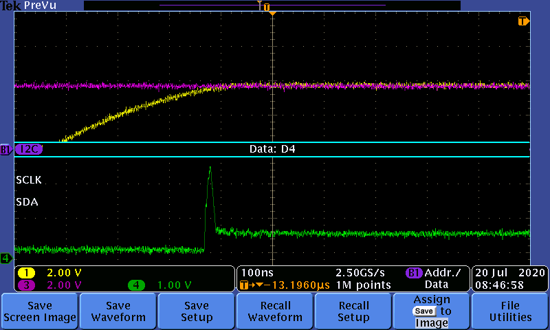
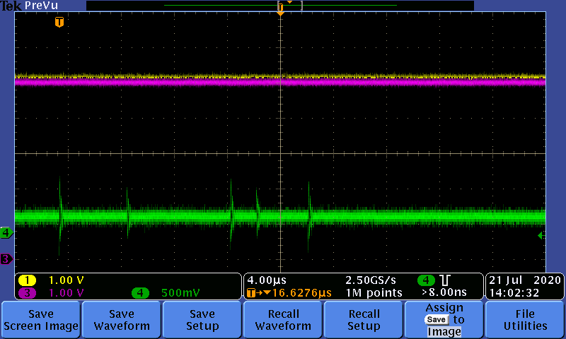
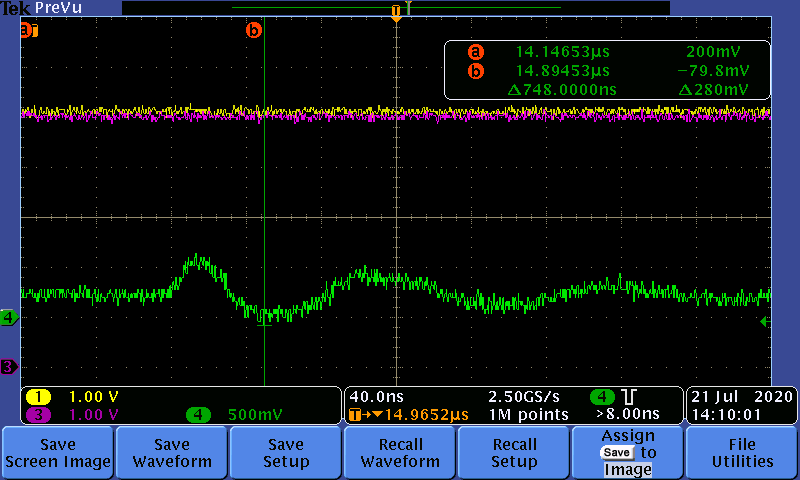
  • Regarding the input signal to ADC channel 3 going below ground, when I look at a board with ADS7828 whose channel 3 is working (no glitch), I see what is shown in the scope traces below -- green signal = ch3 input. First trace has a time base of 4 us / division; second one has time base expanded to 40 ns / division.

    Can transients below ground that are this small (-80 mV at most) damage the device if many of them occur over time as the board operates?

  • Art,

    So if I combine all of the recommendations we've discussed, I get the following list. Is it complete?

    - Drive the ADC channel input with a low impedance amplifier (since the characteristics of the sensor output are not clear).

    - An RC network between the amplifier and the ADC channel input

    - And the Schottky diodes from ADC to Vdd and ADC to ground to prevent electrical overstress

    - And the TVS diode on Vdd to protect against power supply transients.

    Here's something I observed on the power down characteristics --  Vdd (yellow) drops below Vref (purple) and there's a transient on the channel 3 input (green).

    To avoid this, would it be better to use a common voltage for Vdd and Vref?

    Mark

  • I agree.  Power up looks good and power down looks problematic.  I think you found the issue.  I also agree that connecting a common voltage to Vdd and Vref would likely mitigate this issue.   You may also still want a filter between the sensor and ADC.  I suggest trying this and cycling power on your system many times.  Often when we have power supply issues like this, it may show up infrequently.  So, to confirm that the solution is robust using a GPIB controlled power supply and forcing power on and off many times is a good way to confirm robustness.

    Let me know how your testing proceeds.  I hope this solves your issue.

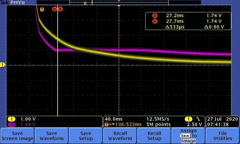
  • We have several inputs on the ADS7828 driven by TI INA331 Instrumentation Amplifiers. The output of each INA331 has a 22uF capacitor to ground and the power down characteristics are given by the scope trace above where the yellow waveform is the supply voltage for both the ADC and amplifier, and the purple waveform is the ADC channel input. Based on our previous discussion, I'm concerned this is another case that would lead to damage of the ADS7828. What would be your recommendation here?

    Regarding the filter you mention in the previous post, I wanted to check on the values for the components. Earlier in our posts you mentioned R=100 ohms, C=1 nF. In our application the ADC inputs vary slowly or are DC only, so the frequency response is not a big concern. Is R=100 ohms, C=1 nF what you would recommend for our application?

    Mark

  • Mark,

    Sorry for the late response.  Yes, I agree with your suggestion.  Placing a current limiting resistor between an amplifier and the ADC can help protect it from overstress.  The capacitor part of the filter can actually slow down the power down of the amplifier, but I don't think this is a real concern as I think the current limit from resistor is the key measure that helps protect the device.  Keep in mind that the absolute maximum input characteristics include a current limit and a voltage limit.  Technically, you should be careful that you do not violate voltage or current limits, but practically it is more important to limit current. 

    We have a couple of really good video series on this subject (links below).  I think you may find some if this information useful. 

    https://training.ti.com/eos-and-esd-adc?context=1139747-1140267-1128375-1139109-1137697

    https://training.ti.com/ti-precision-labs-op-amps-electrical-overstress-introduction?context=1139747-1139745-14685-1138807-13956