This thread has been locked.

If you have a related question, please click the "Ask a related question" button in the top right corner. The newly created question will be automatically linked to this question.

ADS54J66: ADS54j66 Output data

Part Number: ADS54J66

hello,

 we are currently working on ads54j66 in default 4421 mode 8 configuration.Initially we are trying to establish a link between IC and FPGA so we are sending test pattern (counter data) from ADC.

configuration are ;

CLocks (LMK04826B ) ;  ADC clock : 312.5 MHz   sysref : 4.88 MHz    mode : 4421 mode 8(un-decimated)

THE above configuration were simulated on ADS54J66 EVM board and  CUSTOM BOARD board. the  result are as shown below

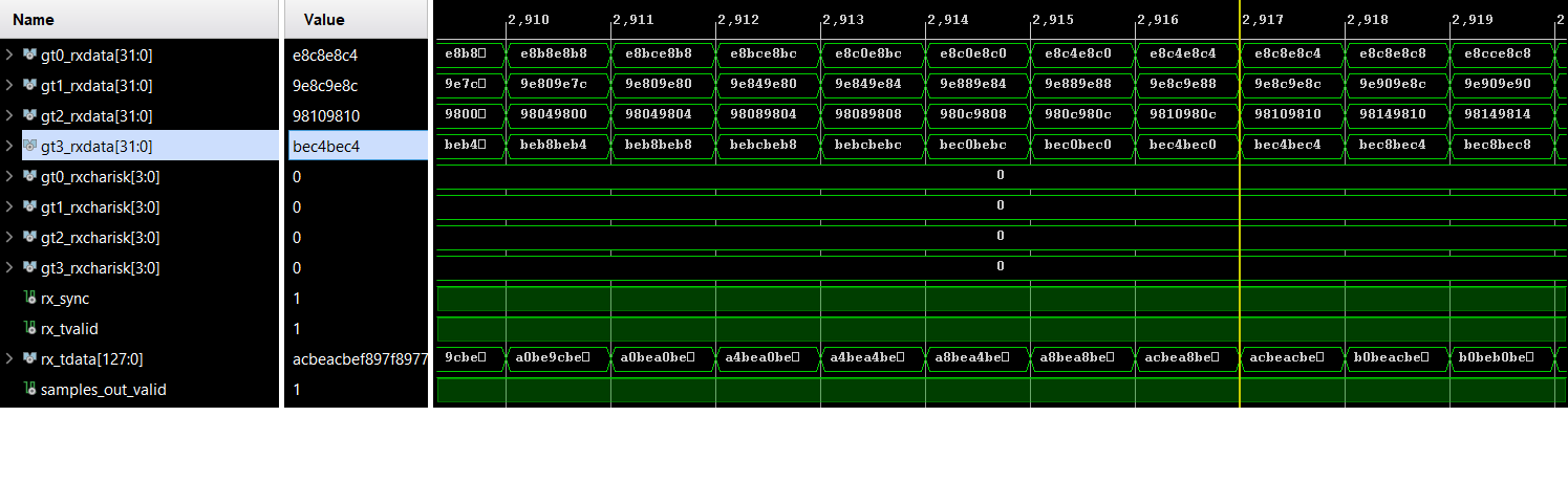
IMAGE 1 : EVALUATION BOARD

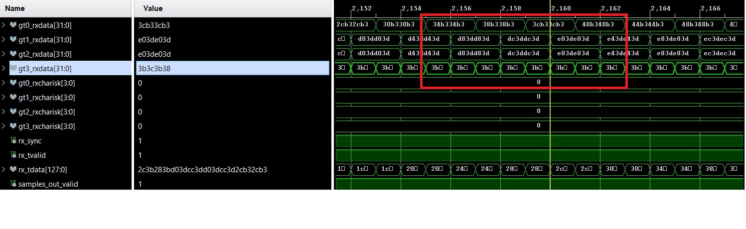
2 : CUSTOM BOARD

for both board LMK configuration, ADC configuration and FPGA configuration are same.

QUESTIONS:

a)  as shown in the second image the counter data is not proper why? when we configure configure ADC with  all zeros test pattern,all ones test pattern and custom patterns ,the output of both boards are same.

b) sometime the counter data is repeating for 3 to clock cycles and den incrementing for sometime and so on.since the behavior is so random we are unable to get to an conclusion. so what are registers which help us to Debug the issue?

thank you

  • THE ABOVE IS RESULT OF EVM  BOARD. THE BELOW IMAGE  IS CUSTOM BOARD

  • User,

    We are looking into this.

    Regards,

    Jim

  • test pattern mode.docxUser,

    Please see attached.

    Regards,

    Jim

  • Hiee jim

     we are writing  the below configuration.So yes we are disabling the DC offset as well.

    0x6068 0x06
    0x7068 0x06
    0x6018 0x03
    0x7018 0x03

    The results of custom board and evaluation board are same when configured as 

    a) all 0's test pattern, b) all 1' pattern c) Outputs toggle pattern d) custom pattern e) de Skew pattern f) sync pattern.

    only for the counter data the behvaior is different as shown in the above images.

  • User,

    I cannot tell what the data is looking at your chipscope capture as there are multiple samples combined. Please send the data in a column format. When capturing the data with the TSW14J56EVM, the ramp is only 14 bits and the two LSB's are noise. Not sure if this is what you are seeing or not. See attached.

    Regards,

    Jim 

    1882.ADS54J66_ramp_test_Mode_8.pptx

  • iladata.csv

    Hello jim,

    Please find the attachment. the data is from custom board and was configured as per the decision in mode 8(undecimated) and disabled DC offset.

    I would like to add one more question .

    as we can see the dataline (GT0...GT4) on EVM Screenshot above,the data is received is in every clock cycle in all lane, but in custom board the data is same in lane GT1 & GT2 but is different in others why?

    The same behaviour is observed on  remaining working ADC on our custom board. can we align the data after completion of ILA phase i.e when we start recieving data?

    Thank you for ur support throughout our so far. 

  • User,

    Sorry but a still cannot understand the data you are sending. Can you  convert it to columns with each column being the data from one lane. Inside the column enter the value in decimal for each sample. Do this for 10 samples are enough to show the problem.  What is different between the EVM and custom board? Are you issuing a hard reset after clocks and power are applied to the ADC? Have you consulted with Xilinx about this? Please send the register settings and in the order you are writing them to the ADC. What FPGA are you using?

    Regards,

    Jim

  • iladata (1).csv

    0x0000 0x81
    0x4004 0x68
    0x4003 0x00
    0x4002 0x00
    0x4001 0x00
    0x60F7 0x01
    0x60F7 0x00
    0x70F7 0x01
    0x70F7 0x00
    0x0011 0x80
    0x0053 0x80
    0x0039 0xC0
    0x0059 0x20
    0x6000 0x01 
    0x6000 0x00 
    0x7000 0x01 
    0x7000 0x00 
    0x4004 0x61 
    0x4003 0x41
    0x6000 0x08 
    0x7000 0x08
    0x6001 0x04 
    0x7001 0x04
    0x4003 0x00 
    0x4004 0x6A
    0x6016 0x02 
    0x7016 0x02
    0x4003 0x00
    0x4004 0x69
    0x6000 0x20
    0x6001 0x01
    0x7000 0x20
    0x7001 0x01
    0x6000 0x80
    0x6006 0x1F
    0x7000 0x80
    0x7006 0x1F
    
    
    # ADC DATA
    
    0x6000 0x80
    0x7000 0x80
    0x6002 0x00
    0x7002 0x00
    0x4004 0x61
    0x4003 0x00
    0x6068 0x06
    0x7068 0x06
    0x6018 0x03
    0x7018 0x03
    
    0x0011 0x0f
    
    0x0074 0x40

    HELLO JIM

    I have sent the configuration reg file and counter data from each lane . please find the attachement.

    when i fed in input data the output level is very high comparative to other ADCs and noise floor is also more. why?


  • Hello jim

    Could  you explain why different lane are reading data at different clock.why this is not similar to EVM board result  as shown in previous conversation

    Thank you

  • User,

    I cannot explain this. Please send you register settings and in the order you are loading them into the ADC. Are you issuing a hard reset after power and clocks are present but before writing to the ADC?

    Regards,

    Jim

  • 0x0000 0x81
    0x4004 0x68
    0x4003 0x00
    0x4002 0x00
    0x4001 0x00
    0x60F7 0x01
    0x60F7 0x00
    0x70F7 0x01
    0x70F7 0x00
    0x0011 0x80
    0x0053 0x80
    0x0039 0xC0
    0x0059 0x20
    0x6000 0x01 
    0x6000 0x00 
    0x7000 0x01 
    0x7000 0x00 
    0x4004 0x61 
    0x4003 0x41
    0x6000 0x08 
    0x7000 0x08
    0x6001 0x04 
    0x7001 0x04
    0x4003 0x00 
    0x4004 0x6A
    0x6016 0x02 
    0x7016 0x02
    0x4003 0x00
    0x4004 0x69
    0x6000 0x20
    0x6001 0x01
    0x7000 0x20
    0x7001 0x01
    0x6000 0x80
    0x6006 0x1F
    0x7000 0x80
    0x7006 0x1F
    
    
    # ADC DATA
    
    0x6000 0x80
    0x7000 0x80
    0x6002 0x00
    0x7002 0x00
    0x4004 0x61
    0x4003 0x00
    0x6068 0x06
    0x7068 0x06
    0x6018 0x03
    0x7018 0x03
    
    0x0011 0x0f
    
    0x0074 0x40

    Hello Jim

    1) I have sent the configuration register file and data in decimal format in my previous post.

    once again i am sending you the configuration register

    2) No i am issuing any hard rest.

    3) yes LMK PLL is locked before configuring ADC registers.

  • User,

    I cannot explain this. Please try the new configuration file I have attached. By default, the part will write to both channel banks (broadcast mode) so you do not need to write to 0x7000 address spaces. 

    Regards,

    Jim

    0x0000 0x81
    0x0011 0x80
    0x0039 0xC0
    0x0053 0x80
    0x0059 0x20
    0x4004 0x68
    0x4003 0x00
    0x4002 0x00
    0x4001 0x00
    0x60F7 0x01
    0x6000 0x01 
    0x6000 0x00 
    0x4004 0x61 
    0x4003 0x41
    0x6000 0x08 
    0x4004 0x6A
    0x4003 0x00 
    0x6016 0x02 
    0x4004 0x69
    0x4003 0x00
    0x6000 0x80
    0x6006 0x1F


  • User,

    You need to issue a hard reset after clocks and power are present. Please try the attached config file.

    Regards,

    Jim

    0x0000 0x81
    0x0011 0x80
    0x0039 0xC0
    0x0053 0x80
    0x0059 0x20
    0x4004 0x68
    0x4003 0x00
    0x4002 0x00
    0x4001 0x00
    0x60F7 0x01
    0x6000 0x01 
    0x6000 0x00 
    0x4004 0x61 
    0x4003 0x41
    0x6000 0x08 
    0x4004 0x6A
    0x4003 0x00 
    0x6016 0x02 
    0x4004 0x69
    0x4003 0x00
    0x6000 0x80
    0x6006 0x1F