This thread has been locked.
If you have a related question, please click the "Ask a related question" button in the top right corner. The newly created question will be automatically linked to this question.
Hi,
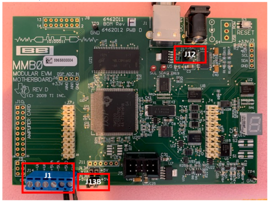
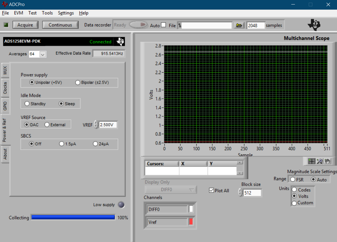
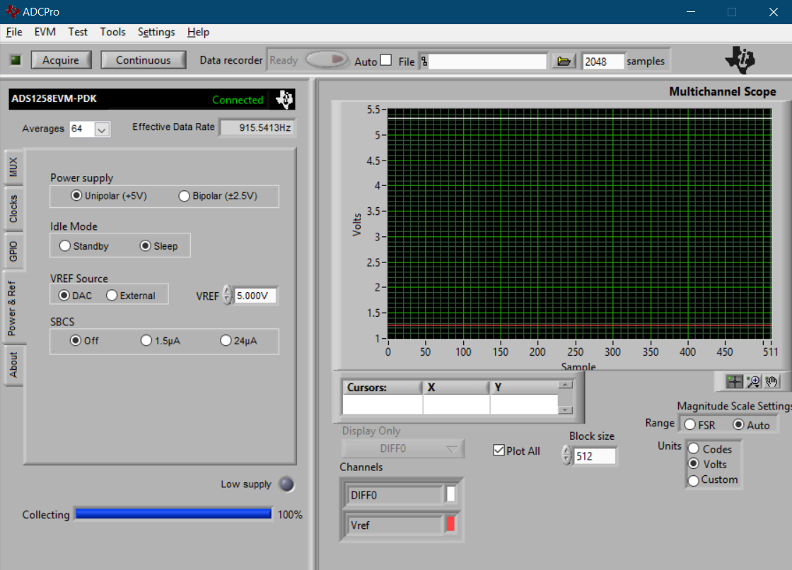
I'm using the ADC pro software and the ADS1258EVM development board.
I've made the following jumper settings: S1 = GND, S2 = DAC and I'm using an external 5V power supply.
In the Power & Ref tab I've set the VREF source to DAC and 2.5V.
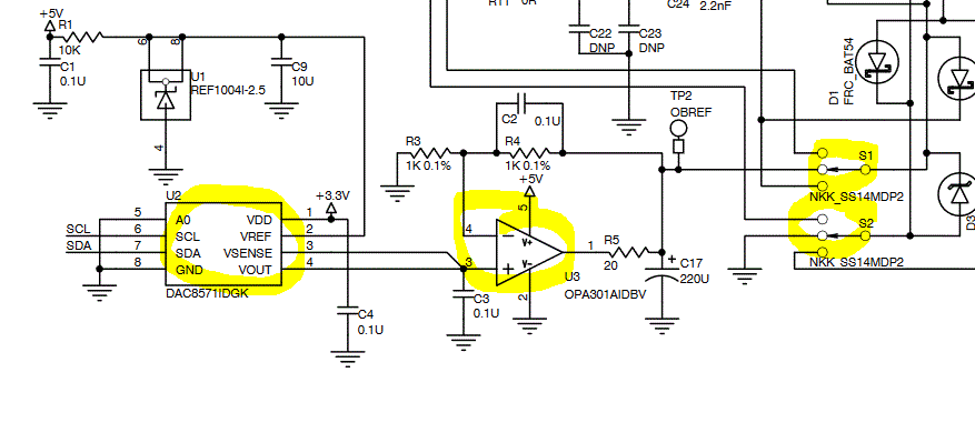
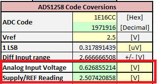
However when I look at the output in the multichannel scope the VREF appears as 0.6V - and is always approximately one quarter the set VREF voltage.
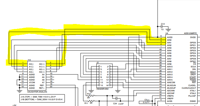
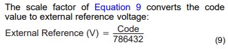
I've noticed on page 8 of the ADS1258EVM-PDF User Guide that it states the output of the DAC is multiplied by 2 - but I don't understand why the output I'm seeing is quatered. Shouldn't I see an output of 2.5V? I also notice a similar effect if I connect the DIFF0 output to Gnd and Vdd, I see half the Vdd voltage.
Could someone point out the setting I have wrong/the gap in my understanding of how it should work?
Hi Mark,
I assume you are measuring the DAC output (VOUT pin) correct? If so, then this should be half of whatever the VREF voltage you set in ADCPro. As you can see from the piece of EVM schematic below, there is a non-inverting amp on the DAC output with a gain of 2. If you measure the voltage at the VREFx pins, you should get 2.5V.
I did not understand the second point about the Diff0 output - can you please add more detail about where you are measuring?
-Bryan
Hi Bryan,
Thanks for taking the time to look at this. I assume I'm just measuring the OBREF point as setting switch S1 (from the schematic in your reply) to the middle setting appears from the schematic to select the output of the op amp.
In my question where I say I measure the output of the DAC using a multichannel scope I'm referring to the inbuilt multichannel scope test tool in the Texas Instruments ADC Pro software.
Similarly, when I select the DIFF0 input in the ADC pro software the measurement is half of what I'd expect it to be. The schematic below shows the connection of the AIN0 and AIN1 (DIFF0) to the output header - which I've simply connected to Gnd and +5V respectively.
I can't see/understand where/why any of the settings I've configured would cause the measured voltages to be halved. The configuration settings (that I believe are relevant) are listed below for both the MMB0 board and ADS1258 daughter board.
J13B = Jumper between 5V and 5VA (+5V is supplied from 5V analogue).Hardware Settings
J1 = 5V and Gnd.
J12 = disconnected (powered through the terminal block).
S2 = Middle – Gnd (Sets Vref negative input to Gnd).
S1 = Middle – DAC (sets Vref positive input to output from DAC).
D4 = Jumper between 1 and 2 – AVDD supply current measurement point for the ADC. Must be connected for operation.
D4 = Jumper between 3 and 4 – AVSS supply current measurement point for the ADC. Must be connected for operation.
D4 = Jumper between 7 and 8 – 3.3V supply selected.
D4 = Jumper between 9 and 10 – DVDD supply current measurement point for the ADC. Must be connected for operation.
D4 = Jumper between 11 and 12 – Connects DGND to board ground.
J1A (1) = Gnd.
J1A (2) = 5V.
Below I've attached some screen captures from ADCPro showing my software setup and the output from the scope.
The clock source has been set to - MMB0 - 16MHz and the External Multiplexor Loop check box has been unticked (which I assume disables the external bypass i.e. the ADC input does not go to an external signal conditioning circuit).
You can see in the image above that VREF output is approx 0.6V and the DIFF0 output is approx 2.6V.
If I adjust the VREF to 5V I get the following.
You can see in the image above that VREF output is approx 1.25V and the DIFF0 output is approx 5.25V.
Hi Mark,
I took a look at this on the ADS1258EVM that I had on hand and was seeing same thing...
What is happening is that ADCPro is collecting the correct ADC codes for the input and the reference voltages, but when converting these codes to voltages for the plot, it is using the same scaling factor for both measurements, resulting in an incorrect reference voltage which is about 1/4-th of the expected value.
From the ADS1258 datasheet, here is the equation for calculating the reference voltage:
For a typical analog input voltage measurement, you'd calculate the input voltage by dividing VREF by 7864320 (a 10x larger factor than the one in equation 9 above, hence 2.5V/10 results in the 0.25 scaling) to calculate the LSB size of the ADC. Then you'd multiply the output code by the LSB size to compute the voltage.
If you look at the raw ADC codes in the data monitor, you'll see the reference voltage measurement producing codes near "0x1E16CC". When you apply the different scaling factors to this code you'll get the following results:
There is Excel calculator on this E2E post that you can download and use to check your output codes: https://e2e.ti.com/support/data-converters/f/73/p/667354/2473257#2473257