


Part Number: ADS52J90
Tool/software: WEBENCH® Design Tools
Hi,
I'm using ADS52J90 to work in 32 inputs mode with JESD204B subclass1 standard. I use it with 4 CML output lanes and 12-bit resolution.
My configuration is that the Octet per frame is 6 or 8. As for 6,Which would mean per single sample shot each lane would output at least (12x4) 48 bits of data.
From the ADS52J90 datasheet, 32 inputs means one ADC needs odd sampling circuit to sample odd channel's input, even sampling circuit to sample even channel's input. Their data bits is in the same position of different frames of 48 bits. As for LVDS mode , we have FCLk for the logic device to receive the serial data ,and distinguish whether the data belongs to odd channel or even channel (as showing in figure 68, page 46).
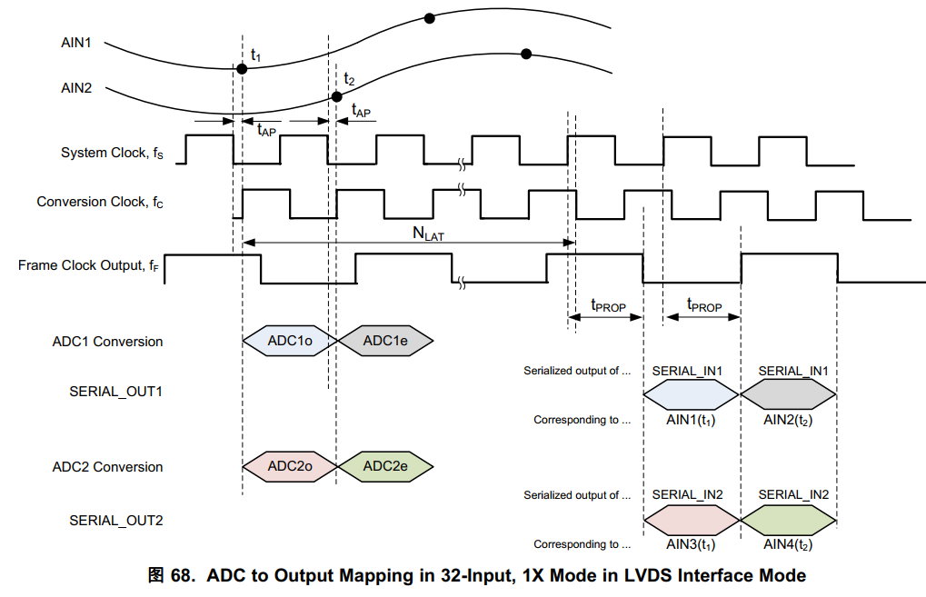
But for JESD CML lane ,when the logic device, such as Xilinx FPGA, uses JESD IP core to receive CML data by frames, how can I know which channel the data in a certain frame belongs to ? I can's find any information from the datasheet.

My conclusion is that , the JESD IP core receives data as shown above(page 22, PG066, Xilinx), the first frame after rx_valid is for odd channel, and the next frame consists the data of even channel. Which means the first frame in one multiframe stands for data of odd channel, and the second one for even.
Is it the real situation,or there is something I miss? And if it's true, when the multiframes contains odd number of frames , We always loss one frame of even channel's data,isn't it?
Thanks
Chen
