This thread has been locked.

If you have a related question, please click the "Ask a related question" button in the top right corner. The newly created question will be automatically linked to this question.

ADS54J40: 4 lanes mode - signal on unused lanes

Part Number: ADS54J40
Other Parts Discussed in Thread: THS4511, ADS54J60

Hello, I have prototype board with ADS54J40 which is connected to the FPGA via FMC+ connector using 8 lanes. Unfortunately one of lanes is connected to wrong FMC+ pin so I am using ADC in 4 lanes mode. JESD is working and I can receive correct data, but there is always 250 MHz in signal frequency spectrum (even with unconnected inputs) which is quarter of the sampling frequency 1 GHz. We tried to change it to 900 MHz which results in parasite frequency of 225 MHz (again one quarter of the sampling frequency). 

On ADC board there is nothing what would generate this frequency. After some elaboration we found out that there is something going on on unused JESD lanes with exactly quarter of sampling frequency. As ADC is in 4 lanes mode I supposed that unused lanes should be powered down but they either aren't or something else is going on.  

Thank you in advance for your suggestions.

  • Jakub:

    It sounds like you may be seeing the interleaving spur that occurs at Fs/4.  Check to see if the spur you are seeing is consistent with the levels outlined in the datasheet specifications.  If so, this spur is expected given the ADC interleaving architecture.

    --RJH

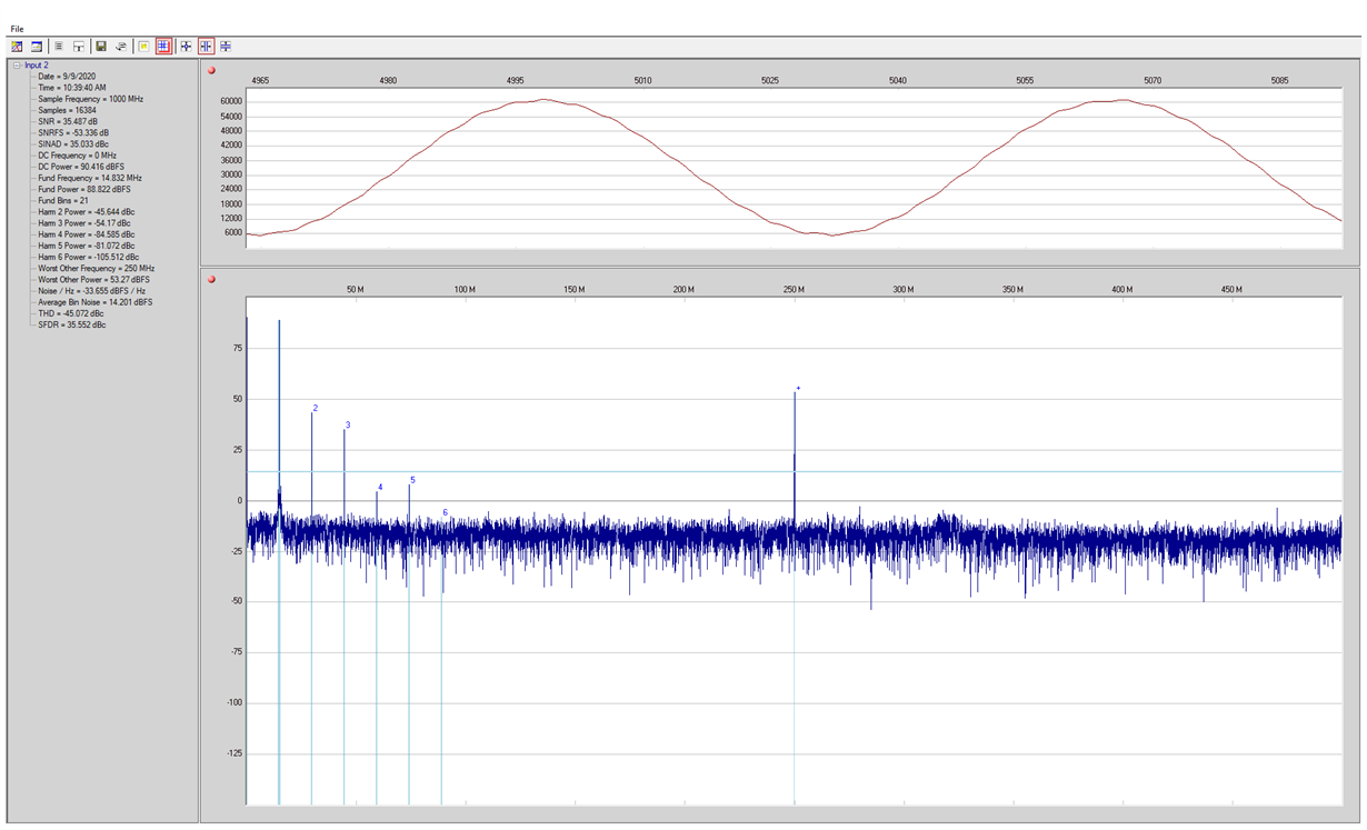
  • This was my firt though too, but the 250 MHz component is only 40 dB from input signal frequency (it is higher than other harmonic frequencies). If I understand it right it  should be according the datasheet between 77 dB to 85 dB considering measured signal frequency.

  • Here you can see sampled signal together with it's frequency spectrum.

  • Hi Jakub,

    One thing that could be an issue is the interleaving correction. Can you check and make sure that the register settings are set correctly for this, such as having the correct nyquist zone selected?

    Regards,

    David C

  • Thank you for reply.

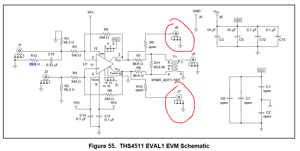
    We left this register unchanged as we are working in the first Nyquist zone. One thing I forget to mention is that we have input drive circut built (shematic bellow) in such a way, it can be used with small changes either as single ended or differential. Schematic is below.

    The thing is when we remove R1 and R7 resistors and use it as single ended the resulting frequency spectrum is as expected according to datasheet - 250 MHz component is about 80 dB below the input signal frequency component.

    If we instead of R1 and R7 remove C1, C2 and C7 and use it as differential the resulting spectrum is as described - 250 MHz component only about 35 dB below the input signal frequency component.

  • Hi Jakub,

    What are you using to drive the differential inputs? Is the differential input being DC coupled, as this could cause an issue?

    Regards,

    David Chaparro

  • Hi David,

    we are using slightly adjusted THS4511 evaluation module to drive differential inputs so it's DC coupled.

    We found some information regarding DC offset correction as it could cause this kind of behavior (large spur on fs/4 and fs/2). In documentation for ADS54J60 is mentioned that the DC correction engine has to be frozen before input signal can be applied. As I understand it ADS54J40 and ADS54J60 has the same (or very simillar) set of registers. For some reason not all of them are mentioned in ADS54J40 documentation.

    Do you know about some kind of configuration sequence which would lead to correct setting of the ADC? We tried to follow steps mentioned in this document (from this answer) but nothing has changed.

  • Jakub,

    I will take a look at the document and see if there needs to be any other settings added.

    Regards,

    David Chaparro

  • Jakub,

    Based on what you are seeing when you use differential inputs you could have a VCM problem. To verify if it is a VCM problem I have a couple of questions:

    • Are you applying the VCM from the ADC to the amplifier?
    • What are the supplies you are using on the amplifier?
    • Are you making any other changes when switching between single ended and differential inputs?

    Regards,

    David Chaparro