This thread has been locked.

If you have a related question, please click the "Ask a related question" button in the top right corner. The newly created question will be automatically linked to this question.

DDC118: Zero offset leve jumps

Part Number: DDC118

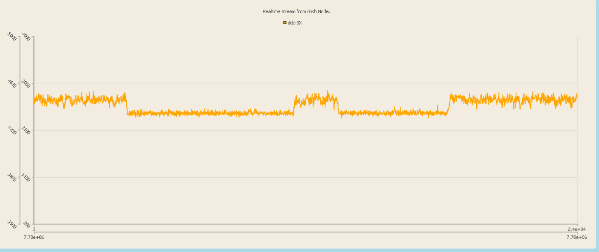
We have a product with a DDC118. Some units shows a behavior where the zero offset level starts at a level and after a period of time start to jump up to a new level. During a transition time the level makes jumps up and down between the levels and after more time the level stabilizes at the upper level. 2 out of 10 units show this behavior. The device is supplied with 5V, 3.3V and 4.096 reference and I can not see any strange on these supplies. The timing requirements for all clocks are fullfilled. The device is clocked at 19.2MHz.

Is this any known issue? See attached graph.

  • Hi Ulf,

    I'm not aware of any known issue for the offset step for the DDC118. It will be helpful if you can provide more information and details as to how the DDC is setup in this case. How is the input connected when you are measuring this offset? If you can give more details on the attached plots (x-axis, double y-axis) so I can understand what your plot is showing. 

    Is it side A or side B? Does this happen on all channels or only on random channel for all the devices that you see? 

    Thanks.

    -TC

  • I attached files of the schematics and a excel file of the data. Channel 1-7 are connected to diodes but channel 8 is not connected. The data attached is from channel 8.

    ddc-ddc.pdf

    DDC118 jump.xlsx

  • Hi Ulf,

    Thank you for the data and the hardware design information. After checking with the team, we haven't seen this issue with the device. In order to help us understand better and to debug the issue, please review and check on a few things listed below.

    1. In your schematic, I see CH8 is not connected in your application and is used to collect this data. For the device that is having this issue, can you also take some data on the remaining channels (CH1-7) by disconnecting the input from the PD?  

    2. Does this happen with different device and hardware setting conditions (supply, CLK, Range, High-Speed/Low-Power Mode, etc) for the board you are seeing this issue? 

    3. Is the offset jump sizes always the same for all the devices that you are seeing this issue? 

    4. Take the device from the board with issue and put it on other board that you are not seeing the issue?

    If you are still seeing the same issue with the device, we can setup something to have the devices shipped back to us for further evaluation and verification. Thanks and please let me know if you have any questions.

    Thanks.

    -TC

  • I found the problem but I don't understand why.

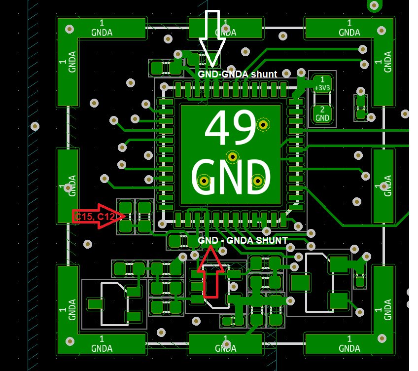
    I changed the capacitors on the reference voltage C22, C12 to capacitors with 0603 package from 04042. This eliminated the problem.

    I have split AGND and DGND at the pins of the DDC. I am not sure if this could cause the problem in combination with a stray resistance in the capacitor. What do you suggest about the GND. Combined DGND and AGND planes or split planes?

  • Hi Ulf,

    It is good to hear that you are able to fix your issue. In the datasheet, we have recommended that both the analog and digital grounds (AGND and DGND) be connected to a single ground plane on the PCB.

    Thanks.

    -TC