This thread has been locked.

If you have a related question, please click the "Ask a related question" button in the top right corner. The newly created question will be automatically linked to this question.

DAC8775: DAC8775 Can't work

Part Number: DAC8775

Hi

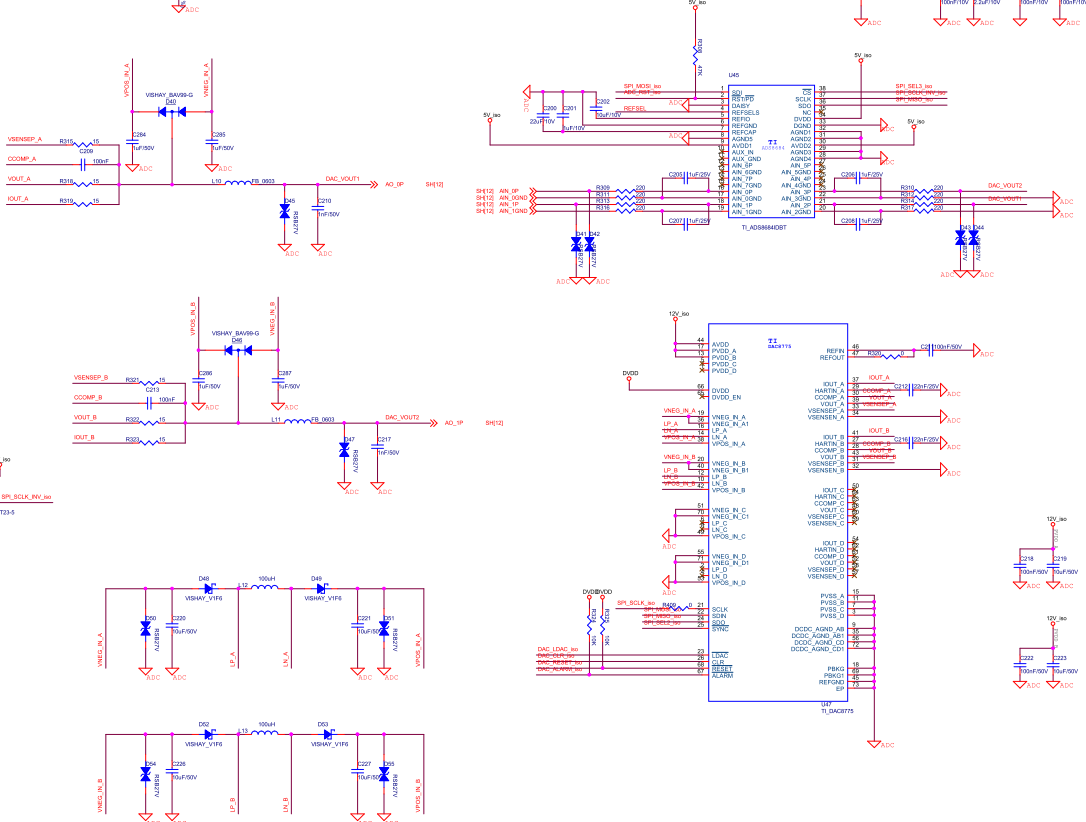
We used the DAC8775 IC for DAC output application.

but some problem need to help,following register setting in the sequence by DAC8775 datasheet

when setting Reg(0x04) = 0x1003;Reg(0x0B)=0x1001;

We can't get right value in voltage mode

I don't know what is causing this problem

Register setting as below.

nRESET = 0;

CLR = 0

nLDAC = 0;

Reg(0x00) = 0x0001;       // reset

Reg(0x02) = 0x0012;       // REF_EN = 1, PCO = 1

Reg(0x06) = 0x0001;       // select Buck-Boost converter A

Reg(0x07) = 0x0000;       // disable Buck-Boost converter A

Reg(0x06) = 0x0002;       // select Buck-Boost converter B

Reg(0x07) = 0x0000;       // disable Buck-Boost converter B

Reg(0x06) = 0x0004;       // select Buck-Boost converter C

Reg(0x07) = 0x0000;       // disable Buck-Boost converter C

Reg(0x06) = 0x0008;       // select Buck-Boost converter D

Reg(0x07) = 0x0000;       // disable Buck-Boost converter D

Reg(0x03) = 0x0020;       // select channel A

Reg(0x04) = 0x0003;       // Range = Voltage output +-10V

Reg(0x05) = 0x8000;       // DAC = 32768

Reg(0x04) = 0x1003;       // Output enable (OTEN = 1)

  • Reg(0x0B).bit 0 reports Fault channel A (FA == 1)

  • nALARM remains high (no alarm)


The DAC8775 related part of schematic as below

some one can help me to figure out the problem?

Thanks

  • Hi,

    The schematics you posted here is not visible. Please reattach schematics using the image attach button in the toolbar.

    Regards,

    AK

  • Hi,


    Looking at the code, I generally don't see anything wrong. One thing that I did note is that a reset is a write of 0x0001 to register 0x01, not to register 0x00. However, I don't think that's the why you don't have the correct output.

    First, it looks like you have disabled all of the buck-boost converters. Do you have external supplies on VPOSx and VNEGx? It is ok if you do have external supplies, but make sure you keep the buck-boost converters OFF, or you may damage the device.

    The DAC error that you have in 0x0B seems to indicate that the DAC output is in error. In this case, it might mean there's something wrong with the power, or you have something in the circuit mis-configured. As Akhilesh mentioned, it would be good to post the schematic. When you do post the schematic, you cannot cut and paste an image into the post. You will need to use the "Insert/Edit Media" picture icon to add a picture.


    Joseph Wu

  • Hi Akhilesh K

    I posed my schematic as below,please help me to check.

    This design is +/-10V voltage output and 0~20ma current output

    by the way, i am so confusion that the voltage and current in same trace,so how can i check that the current output is correct by my setting?

    for example, when i setting different current output value,i can still measure the different voltage in same node? right?

  • Hi Joseph

    thanks for your reply

    i already reattach a part of schematic

    two DAC output are feedback to ADC input for monitor, if this design have any Inappropriate ,please help us to find out it.

  • Hi,


    For your system, it looks like you're using the Buck-boost converter for channels A and B. I would enable the buck-boost converter, and set it to enable the PCLMP and NCLMP for the CCLP bits and then set the clamps to +15V and then -15V. This should enable the buck boost to put that voltage to VPOSx and VNEGx.

    That should allow for the VOUT mode of the DAC. After that you can set up the DAC as you would to output something in voltage mode.

    Once you have this programmed, check the output voltages of the VPOSx and VNEGx. If that appears correct, then check the VOUT of the DAC. Note that with IOUT mode, this may change the VPOSx and VNEGx settings as the IOUT changes. 

    Joseph Wu

  • Hi Joseph

    following your mention before, when i useing the buck-boost converter

    and setting PCLMP and NCLP for -15V~+15V rang ,then check VPOS_A and VENG_A

    No matter what i change another level,only setting NCLP is correct by measure VENG_A

    VPOS_A seems keep around 22.3V whatever i set +9V or +15V as below picture

    Of course i still can't get right value by DAC output in voltage mode.

    So what is next step by your suggestion

    Ch1. VPOS_A (green)

    Ch2. VNEG_A (blue)

  • Hi,


    I would try to verify the write to the device. At this point the output voltage of 22.3V for VPOS_A is unusual for a voltage output and the clamp shouldn't work at to that setting. However, at the current output mode, you may get different VPOS settings for different current outputs depending on the load resistance and what headroom you might need for the output.

    Try setting the registers and reading them back to verify that the write has taken place correctly. I would read back all of the registers just to ensure that the setting is correct. Normally, by setting and enabling the range to a voltage output setting, the buck-boost converter will automatically set the buck-boost to the ±15V settings.


    Joseph Wu