This thread has been locked.

If you have a related question, please click the "Ask a related question" button in the top right corner. The newly created question will be automatically linked to this question.

ADS8686S: ADS8686 ADC outputs repeated readings of the first sequence

Part Number: ADS8686S

We employ a ADS8686 16 ch ADC in one of our designs. Most of the time the ADC reads the entire sequence of channels properly. However, occasionally it appears to read one sequence only and repeats that sequence reading instead of reading all channels. I'm not sure what is causing this or how to reproduce it reliably. But once it starts repeating the seq0 readings in stays in that mode.

Background:

Analog VDD=5 VDC, Digital VDD=3.3 VDC, schematic attached.

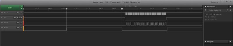
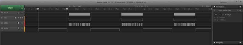
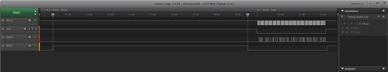
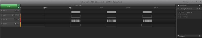
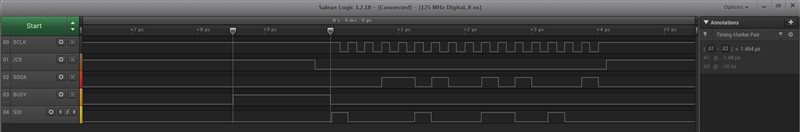
Out HW has configured the ADS8686 to operate in serial SPI, 1 wire mode.  The chip goes through a long reset at power up. We run the SPI bus @ 4 MHz and are able to program the config registers to run in SW configured sequence of 5 sequences that are read back with one CONVST in Burst mode.  I have confirmed that the sequence configuration is correct by reading back all programmed registers and confirming that the values read back match the programmed values. The configuration register contents remain correct even when the ADC readings are bad. At no point do we reset the chip after the initial configuration. At the end of the initial ADC configuration, we do a dummy ADC reading of our entire sequence of 10 ADC channels and confirm that the data read is proper. We can tell this because Ch4A is programmed to always output 0xAAAA, and when the readings are good, this channel reads 0xAAAA as expected.  I have (see the SPI timing screen shot attached. BTW: the CLK signal going to the ADS8686 is actually inverted from what is shown on the Saleae screen shot.)

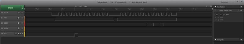
Once initialized the subsequent ADC readings also produce expected results. However after a some time and for an unknown reason, the ADS8686 starts returning 1 sequence worth of data which repeats 5 times during our read. In fact, even the one sequence data appears to be very close to the CH_A0 data that is repeated for CH_B0 and the subsequent CH_AX & CH_BX values. (when accounting for the different ranges that CH_As and CH_Bs had.)  I have confirmed that when the ADC readings are bad (repetitive CH A0 ) that the SPI readings and CONVST, BUSY timing on the scope are the same as the normal reading case. Jus the data contents are garbage.  

My ADC initialization and readADC functions are both attached.

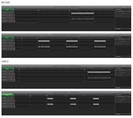
We also found out that if we generate two successive CONVST pulse and wait for the BUSY line to indicate “conversion complete”, then our intermittent read problem frequency gets harder to reproduce. But we don’t quite know why nor can we be sure that this is a real solution to our problem.

Thank you for your help,

Fred

ADS8686.pdfADS8686_Timing.pdf


ADS8686_SourceCode.txt
void InitADC(void)
{
unsigned char cmd[2];
unsigned char txBuf[ADC_COUNT * 2];   // First byte = read cmd, rest = garbage
   

   // Ensure that we get a FULL RESET (> 1.2 uS) since InitIO call put us in reset
   DEASSERT_ADC_RESET;
   // First real CONVST must wait 15 mS AFTER the reset is De-asserted
   __delay_cycles(DELAY_100US);

   // SW Mode Sequencer Configuration Steps(From ADS8686S manual section 7.4.2.5.2)   
   
   // Step 1: Program the Analog Input range for each channel. We use A0-A4 & B0 - B4.
   // All channels use a 10 V range which is the default range. So no additional init is required.
    
   // Step 2: Program the sequencer stack registers to selectc sequence channels
   // Seq_stk_0 is already ADC_CH_A0 & ADC_CH_B0 after reset

   // configure the ADC_REG_SEQ_STK_0
   cmd[0] = ADC_WRITE + ADC_REG_SEQ_STK_0;   
   cmd[1] = (ADC_CH_A0 + ADC_CH_B0 );   
   gpSpiTxBuf = cmd; 
   WriteGPSPI(GS_BLD_ADC);      // Write the Register 
   
   // Start by configuring the ADC_REG_SEQ_STK_1
   cmd[0] = ADC_WRITE + ADC_REG_SEQ_STK_1;   
   cmd[1] = (ADC_CH_A1 + ADC_CH_B1 );   
   gpSpiTxBuf = cmd; 
   WriteGPSPI(GS_BLD_ADC);      // Write the Register
   
   // configure the ADC_REG_SEQ_STK_2
   cmd[0] = ADC_WRITE + ADC_REG_SEQ_STK_2;   
   cmd[1] = (ADC_CH_A2 + ADC_CH_B2 );   
   gpSpiTxBuf = cmd; 
   WriteGPSPI(GS_BLD_ADC);      // Write the Register 

   // configure the ADC_REG_SEQ_STK_3
   cmd[0] = ADC_WRITE + ADC_REG_SEQ_STK_3;   
   cmd[1] = (ADC_CH_A3 + ADC_CH_B3 );
   gpSpiTxBuf = cmd; 
   WriteGPSPI(GS_BLD_ADC);      // Write the Register

   // configure the ADC_REG_SEQ_STK_4. Note CH_A4 is not used. 
   // Step 3: Add the SSREN marker for the last sequence
   cmd[0] = ADC_WRITE + ADC_REG_SEQ_STK_4 + SSREN;   
   cmd[1] = (ADC_CH_A_AAAA + ADC_CH_B4 ); // Note that A4 is used as a test input
   gpSpiTxBuf = cmd; 
   WriteGPSPI(GS_BLD_ADC);      // Write the Register

      // Step 4: Set SEQEN in the config register
   cmd[0] = ADC_WRITE + ADC_REG_CONFIG;   
   cmd[1] = SEQEN + OSR_2 + BURSTEN;   
   gpSpiTxBuf = cmd; 
   gpSpiTxCount = 2;
   WriteGPSPI(GS_BLD_ADC);
   
   // Step 5A: Provide a dummy CONVST pulse
   ASSERT_CONVST;
   txBuf[0] = ADC_READ; // Adding an instruction inbetween to ensure CONVST pulse is long enough
   gpSpiTxBuf = txBuf;  
   DEASSERT_CONVST;
   
   while(P2IN_bit.P2IN6);        // Wait till conv completes.
   
   // Step 6: Assert another CONVST then read back the conversion results
   ASSERT_CONVST;
   gpSpiRxBuf = adcResults; // Adding an instruction inbetween to ensure CONVST pulse is long enough
   gpSpiRxCount = (ADC_COUNT * 2);   
   DEASSERT_CONVST;
   
   while(P2IN_bit.P2IN6);        // Wait till conv completes.

   ReadGPSPI(GS_BLD_ADC);  // Reading all 5 sequences in BURST mode

   // Look for unexpected results
   if ( (adcResults[16] != 0xAA) || (adcResults[17] != 0xAA))
      __no_operation();     // For Debug breakpoint only

}

// This is the example of ADC reading with 2 CONVST pulses. Normally only one CONVST is applied.
void  ReadADCs(void)
{
unsigned char txBuf[ADC_COUNT * 2];   // First byte = read cmd, rest = garbage

   readADCError = false; 
   ASSERT_CONVST;    // Conversion starts at the CONVST rising edge
   gpSpiRxCount = (ADC_COUNT * 2);  // Put other instructions here while converting
   gpSpiRxBuf = adcResults;     
   DEASSERT_CONVST;
   while(P2IN_bit.P2IN6);        // Wait till conv completes. (BUSY pin)
   
   // CONVST needs to stay asserted only 50 nS. Measured to stay asserted for at
   // least 275 nS with the one instruction inbetween
   ASSERT_CONVST;    // Conversion starts at the CONVST rising edge
   txBuf[0] = ADC_READ;; 
   gpSpiTxBuf = txBuf; // Contents of TXBuf can remain garbage.
   DEASSERT_CONVST;
   while(P2IN_bit.P2IN6);        // Wait till conv completes.
   
   ReadGPSPI(GS_BLD_ADC);		// Call the SPI IO handler with SPI CH name
   
   // Look for unexpected results
   if ( (adcResults[16] != 0xAA) || (adcResults[17] != 0xAA)) 
   {
     memset(adcResults, 0x00, ADC_COUNT * 2);
     readADCError = true; 
   }
 
   __no_operation();     // For Debug breakpoint only

}

////////////////////////////////////////////////////////////////////////////
// The header file contents:
// ADS8686 ADC Register definitions
#define  ADC_READ          (0x00)
#define  ADC_WRITE         (0x80)

#define  ADC_REG_CONFIG    (0x02 <<1)
#define  ADC_REG_CH_SEL    (0x03 <<1)
#define  ADC_REG_RNG_A1    (0x04 <<1)
#define  ADC_REG_RNG_A2    (0x05 <<1)
#define  ADC_REG_RNG_B1    (0x06 <<1)
#define  ADC_REG_RNG_B2    (0x07 <<1)
#define  ADC_REG_STATUS    (0x08 <<1)
#define  ADC_REG_ORS_A     (0x0A <<1)
#define  ADC_REG_LPF_CONF  (0x0D <<1)
#define  ADC_REG_DEV_ID    (0x10 <<1)
#define  ADC_REG_SEQ_STK_0 (0x20 <<1)
#define  ADC_REG_SEQ_STK_1 (0x21 <<1)
#define  ADC_REG_SEQ_STK_2 (0x22 <<1)
#define  ADC_REG_SEQ_STK_3 (0x23 <<1)
#define  ADC_REG_SEQ_STK_4 (0x24 <<1)
#define  ADC_REG_SEQ_STK_5 (0x25 <<1)
#define  ADC_REG_SEQ_STK_6 (0x26 <<1)
#define  ADC_REG_SEQ_STK_7 (0x27 <<1)
#define  ADC_REG_SEQ_STK_8 (0x28 <<1)
#define  ADC_REG_SEQ_STK_9 (0x29 <<1)
#define  ADC_REG_SEQ_STK_10 (0x2A <<1)

#define  ADC_IN_RNG_2P5    0x01 // +- 2.5 V Range
#define  ADC_IN_RNG_5      0x02 // +- 5 V Range
#define  ADC_IN_RNG_10     0x03 // +- 10 V Range

// ADC_REG_SEQ_STK_? Regs:
#define  ADC_CH_A0         0x00
#define  ADC_CH_A1         0x01
#define  ADC_CH_A2         0x02
#define  ADC_CH_A3         0x03
#define  ADC_CH_A4         0x04
#define  ADC_CH_A5         0x05
#define  ADC_CH_A6         0x06
#define  ADC_CH_A7         0x07

#define  ADC_CH_B0         0x00
#define  ADC_CH_B1         0x10
#define  ADC_CH_B2         0x20
#define  ADC_CH_B3         0x30
#define  ADC_CH_B4         0x40
#define  ADC_CH_B5         0x50
#define  ADC_CH_B6         0x60
#define  ADC_CH_B7         0x70

#define  ADC_CH_A_AVDD     0x08
#define  ADC_CH_B_AVDD     0x80

#define  ADC_CH_A_ALDO     0x09
#define  ADC_CH_B_ALDO     0x90

#define  ADC_CH_A_AAAA     0x0B
#define  ADC_CH_B_5555     0xB0

#define  SSREN             0x01

//Config Reg:
#define  SDEF              0x80 
#define  BURSTEN           0x40
#define  SEQEN             0x20
// Bits 4-2: OSR
#define  OSR_0             (0x00 <<2)  // No oversampling / OS Disbaled
#define  OSR_2             (0x01 <<2)
#define  OSR_4             (0x02 <<2)
#define  OSR_8             (0x03 <<2)
#define  OSR_16            (0x04 <<2)
#define  OSR_32            (0x05 <<2)
#define  OSR_64            (0x06 <<2)
#define  OSR_128           (0x07 <<2)

#define  STATUSEN          0x02
#define  CRCEN             0x01

// The ADC sequence conversion order

#define  AIN_0A            0 
#define  AIN_0B            1
#define  AIN_1A            2
#define  AIN_1B            3
#define  AIN_2A            4
#define  AIN_2B            5
#define  AIN_3A            6
#define  AIN_3B            7
#define  AIN_4A            8
#define  AIN_4B            9

  • Hi Fred,

    Your schematic was missed, please check. I have few questions:

    1. When the issue happened, were the data on CH_A0 and CH_B0 always repeated 5 times?
    2. Is the BUSY high same between normal data output and incorrect data output/sequence? what's the BUSY high width under both situations?
    3. What's your CONVST width?
    4. What's sampling rate (period time of CONVST)?

    Thanks.

    Regards,

    Dale

  • Hi Dale,

    Here are the answers to your questions:

    1. Yes. Though when I re-ran the problem today I saw a slightly different manifestation in that a 2 byte vale and a 6 byte value are repeated over my 10 readings. Please see the attached pdf file for more details.

    2. No. In a good read busy signal is about9 uS. In a repeated read it is about 500 nS.

    3. I’ve inserted various instructions in between the assert and De-assert to make this width a bit longer. It measures around 400 nS. I believe that the spec is 50 nS.

    4. There will eventually be a 1HZ periodic reading, but these errors are occurring during HW testing which is invoked by a tester. So long times between the consecutive calls. During the specific test that produces duplicate results, there are two consecutive ReadADC calls. So the time between those reading (_CS to _CS)  is about 12.5 uS. However, the first call returns the duplicated values as well as the second call, just a different pattern. (See ADS8686 timing 2 file attached.)

    Re-attached the schematic pdf.

    Finally, I noticed that when the readings are  repeated, my ADC registers do not all contain the values that I expected. The data sheet appears to be silent (don't care) about the contents of MOSI transmission  to the ADC during a read ADC data operation. I am worried that I may be accidentally corrupting the registers during the read. Can you please confirm this.ADS8686 timing 2.pdf7776.ADS8686.pdf

  • Hi Fred,

    Regarding your concern and timing at the end of your post, your SER1W is connected to high in your schematic, so the serial output is available on SDOA and SDOB(2-wire serial mode). The conversion results from channel AIN_0A to channel AIN_7A appear on SDOA, and conversion results from channel AIN_0B to channel AIN_7B appear on SDOB. However, your SDOB is floating, so all data for AIN_xB are missed. The data on MISO in your timing are data only for AIN_xA channels. Also, I do not know why you are sending 10x(8+8) SCLKs to the ADC, actually only 8x(8+8) SCLK clocks are needed for retrieving the data for AIN_xA channels. 500ns BUSY high means no oversampling, you can check if this matches your register configuration. Also, what's your analog input for the test?

    2. Did you change your oversampling configuration? 500ns BUSY high means no oversampling. 9us is incorrect. I suggest no oversampling for all tests and it will make the debug easier.

    4. I would suggest to make the test simpler by using a consistent pattern and sampling rate.

    Also, 0.1uF capacitor can be used for C130 on REFIO pin.

    Best regards,

    Dale

  • Hi Dale,

    1A. I am sorry but I sent you a down rev schematic. In reality both SER1W and SEQEN pins are connected to ground and not to DVDD. That explains why we see real CHB data on SDOA.

    1B. As for sensing 10 WORD (8+8) reads, we use 5 sequences (SeqStk0 – stk4) to read both CHA & CHB inputs, so that’s 10 word reads. Maybe the confusion about SER1W pin contributed to this? If reading only CHA inputs why not read only 5 words? Am I missing some other reason why you think that we should only read 8 words?

    2. I have programmed the config register with an OSR of 2 samples for all cases. When the data is valid (10 unique readings)  the BUSY time is ~9.2 uS. When the data is invalid (duplicated values), the BUSY time is 500 nS. I expect that there still be an oversampling of 2 in the 500 nS case since that parameter is not changed after configuration. What does a 500 nS BUSY and OSR=2 say about the number of actual conversions? Does that mean only one, two or 10 channels were converted during that time?  I am also not sure what you mean by “9uS is incorrect.” Is that too long for 10 sample with an OSR = 2?  Please elaborate.

    4. We used to run with no oversampling (OSR = 0) but we still saw the same problem. I don’t think that OSR has anything to do with this, but since you say that it could make the trouble shooting more straight forward, I’ll do it. What data do you want me to report back to you?

    5. I passed on your recommendation of 0.1 uF ref cap to our HW team. Thanks for the feedback on this.

    6. Finally, you did not respond to my question about the transmit buffer contents being 0 or left as garbage during the data read back. Is there any change of accidentally writing to the config register during the read back?

  • Hi Fred,

    1. 10 WORD (8+8) data reading means you are only using 10 channels of total 16 channels. I tried to confirm with you.

        Except the SER1W,  connecting SEQEN to ground is correct because you are using serial interface in software mode.

    2&4. The 500ns BUSY high for no OSR is incorrect, 9us for OSR 2 is correct. I apologized to make you confused. Please see the following timing plots for SCLK,/CS,SDOA and /BUSY I captured on EVM: serial interface, software mode, SDOA only, Burst sequencer for 5 channel pairs.

    The BUSY high is 4.328us without OSR and the BUSY high for OSR 2 is 9.156us.

    6. Since you could get correct results, I was wondering some possible reasons to cause your issue sometimes, could you please check

    • check without burst just sequencer?
    • Send continuous SCLK clocks or per word to the ADC?

    Also, how many devices or boards showed this behavior?

    Thanks and regards,

    Dale

    NO OSR:


    OSR=2:

  • Hi Fred,

    I think your sequencer configuration was changed and lost for some reasons when the issue happened, the sequencer did not work as expected and only CHA0 was selected and converted. The SCLK clock in #6 may not be the root reason but just wanted to verify. Thanks.

    Best regards,

    Dale

  • Hi Dale,

    Thank you for your response. As I look at your values, they mirror my measurements on my system very closely as follows:

    BUSY_time_OSR2:  9.22 uS & 1.52 us (for the good & bad cases respectively.)

    BUSY_time_OSR0:  1.52 uS & 0.52 us (for the good & bad cases respectively.)

    I had chosen OSR2 since my SPI is a lot slower than your SPI and the majority of time for me is data transmission (77.25 uS & 75.75 uS for the good & bad cases respectively). I don’t think that OSR selection is the issue here.

    The problem that we see is not unique to one unit and happens on all 3 of the ADC PCBs that we currently have.

    I agree with you in that the somehow my sequencer configuration is corrupted. But not certain how. Can you add the chip SDI line to your Saleae screen shots of data reads? I am wondering if your SPI TXBuf is zeroed ahead of time or is left uninitialized. You could even re-progrom the TXBuf with a different sequencer (like add the SSREN bit to the first sequence) and see if the sequence registers are affected by the data read command after CONVST. That would confirm that an uninitialized TXBuf can accidentally reprogram the sequence registers.

    Thanks,

    Fred

  • Fred,

    The purpose to suggest OSR 0 is simplifying the timing for test, I did not think the issue is related to the OSR selection. For same reason, I suggested to use only sequencer without Burst mode for test.

    Below is the timing for sending command on SDI to enable Burst Sequencer mode, FYI.

    Best regards,

    Dale

  • Hi Dale,

    It looks like you do not zero out the MOSI data before reading the ADC CONVST results. (You write 0x8464 read back 0x1A51). Could you configure your ADC channels 15 & 16 to readback 0xAAAA 7 0x5555 and then do a repetitive Burst sequence readback of all 16 channels and ensure that those channels continue to readback as expected. This reproduces our use scenario.

    Zeroing our the MOSI TX buf was the only thing that we did that appeared to have solved our problem, but now the data that you're showing seems to indicate that this should not have helped.

    Thanks for trying this for me one last time,

    Fred

  • Hi Fred,

    Writing 0x8464 to the ADS8686S was used to select Burst sequencer and also configure OSR=2, this is correct, the data read back was not used to read back same register because the command can not be executed in the same frame. I used the EVM GUI for the tests which is very limited so I can not do any test we want including the test you expected. I do not know what "Zero out" you are talking, however it's important to check your timing capture on your board with your software so that we can find something incorrect. Thanks.

    Best regards,

    Dale

  • Hi Dale,

    When you read back the converted data on the SPI line following a CONVST, you have to transmit something on the MOSI (SDI) line while you read back on the MISO line (SOA) line. When I talk about zeroing out the transmit line, I am talking about making sure that the transmit buffer (SDI) contains only 0s while attempting to read back the conversion data on the SDOA line. It is this SPI sequence of reading back the conversion data that I am interested in seeing, and not the configuration of the chip. Sorry if this was not clear before. Showing the chip configuration steps does not help me.

    From what you say, you use the EVM GUI to read back the conversion data. I don't understand why you can't keep your Salaea pins on the 8686 SDI, SDOA, _CS and Clk lines and still capture what the EVM GUI sends to the chip.

    Alternatively, you can share the source code of the EVM where the ADC read is performed, and I can reverse engineer what is being done. This is probably a good thing to include with the EVM kit (which I also purchased) so the end user has one example of how to properly interface with the chip. It doesn't make sense to hide this stuff from your customers. Finally, if you have any example code for any processor that shows an example of how to properly extract the conversion data from the ADS8686 (or any other chip in it's family that operates the same way), that would be very helpful also.

    Fred

  • Hi Fred,

    1. The "Zero out" you are talking about is "NOP" command to just send out clocks to the ADC which is normally used to read from the ADC. The timing I showed just for writing a command to configure the ADC. Below is another timing which was captured for wiring a command to the ADC and the command is a register read command, the 2nd frame shows the register data which is correct as expected. In the 1st frame, we can not send "NOP" command (Zero out) to the ADC because we have to send a register reading command to the ADC. In the 2nd frame, a "NOP" (Zero out) was used to clock out the register data.

    2. If you look at the EVM GUI, it includes separated pages for capturing data and register writing/reading, so either capturing data can be done in the Time Domain page which does not need to send a command to the ADC, or register writing/reading can be done in the Register Map page. Both can not be combined together. This is the reason the experiment you wanted can not be implemented in the GUI.

    3. There is no source code for the GUI because it was developed with LabVIEW. 

    Therefore, it's good to make your timing simple with minimum configurations, then run them to check.

    Best regards,

    Dale

  • Hi Dale,

    Thank you for your prompt reply. I appreciate it. Unfortunately, I can't provide a simplified timing configuration with "No Burst" timing dataq because my ADS8686 is hard wired to have a the Burst Mode enabled (see the schematic previously sent.), and that is the mode that it would have to work in the final product.  However, I fail to understand why you think that the simplified timing would tell us anything different than we already know: We have already confirmed that the conversion (busy high) times on both units is comparable for single and multiple sequences with various OSRs.

    The way I see it, the only question remaining is this: Is it possible to accidentally re-program the configuration registers after the CONVST and during data read portion or not? Typically this is specified in the device data sheet. In this case it is not. Another way to address it is give the customer a sample interface code, which TI does not as far as I know. And I still don't understand why the labview code can't be shared?

    If we keep shortening the read lengths (simplifying the code) we have less opportunity to accidentally overwrite the config registers. That is why I suggested that you purposely fill your "read data" transmit buffers with a wrong init code and see if in fact it corrupts the configuration.

    You almost showed the data that I am looking for in a previous thread from 11 days ago where you showed your SDOA data for OSR0 & OSR2. (see picture below) If you could just capture the SDI data line along with the SDOA & CLK in either of those examples, that would answer my question also.

    Thank you for your assistance,

    Fred

  • Hi Fred,

    If your timing meets the requirement to program the register, "accidentally re-program" could happen. For example, writing 10000100 00000000b  will disable sequencer and burst, which requires only two pulses on proper locations with SCLK clocks. This should be the case for you because your ADC worked well at the beginning and the issue happened after it worked for some time. It may be caused by an interference signal in your case.

    As I said, LabVIEW is not written with code, you will understand if you are familiar with it. I used the GUI software to capture the data and the GUI can be downloaded from here, the GUI can not be modified.

    The timing graph I shared yesterday has included the data captured on the SDI and SDOA&SCLK, is this not what you want? I can not modify the timing to do more experiments because the GUI can not be modified.

    Since your ADC and software worked at the beginning and it was affected by interference signal later, so the hardware mode on ADS8686S should be the best mode for you because it's more robust. 

    Regards,

    Dale

  • Hi Dale,

    You are correct. Your timing graph from 2 days ago did contain SDI and SDOA, but it only showed device configuration and not a CONVST followed by ADC data read. It is SDI during the data read that I am interested in.

  • Hi Fred,

    As I explained 3 days ago, I can not modify the GUI to generate the timing you wanted. Either capturing data can be done in the Time Domain page or register writing/reading can be done in the Register Map page in the GUI.

    Regards,

    Dale

  • Hi Fred,

    As a reminder, the SDI is only required when writing or reading registers. It's not needed when reading conversion data, see the timing in figure 73 and 74 in the datasheet. Usually the controller only needs to send "NOP'(all zeros) on SDI for sending clocks on the SCLK. so you will only see all zeros on the SDI when reading conversion data.

    Regards,

    Dale

  • Hi Dale,

    Figures 73 & 74 of the data sheet do not show the SDI line. In fact, no where in the data sheet that I could find is there a requirement to  NOP the SDI line during conversion data read. This leads the reader to think that the SDI contents during read is a "don't care" instead of NOP as you suggest that the controllers "usually" send.

    If transmitting NOP on SDI during conversion data read is required and  guarantees that the configuration registers are not corrupted, I would like to you to confirm that, and then we can close the thread. But I don't want to assume this is the root cause and then later find my configuration registers are corrupted again for a different reason.

    Thank you for your time,

    Fred

  • Hi Fred,

    These figures do not show signal because they do not need it for reading conversion data. The data sheet could be more clear in the future.

    Our ADCs including ADS8686S do not need NOP (all zeros) command. The only reason you have to send out NOP command is your microcontroller or CPU, they need to send something for sending out the clocks on the SCLK. If you use FPGA, you do not need to send NOP (all zeros) command because FPGA can send out clocks without sending any data or command on SDI line.

    The content of your configuration register could be changed by interference signal or glitch to the SDI, this is possible if you have a harsh electrical environment.

    Regards,

    Dale

  • I wanted to close the loop on this problem for those who may experience this same issue in the future. We found two problems that stem from ambiguous data sheet specification that led to our problems. These are:

    1. After the CONVST signal has been asserted and the data is being read (in our case 1 channel SPI interface), the SPI transmit buffer must be cleared. If it is not, and the msb bit is set on any byte, this could be interpreted by the ADC as a write command and can corrupt the previously programmed chip configuration. Clear the transmit buffer to all 0s before any read attempt.

    2. Reading back the chip configuration registers can not be terminated with a real register read as the data sheet states can be done. If you do that then the contents of that register will remain on the ADC chip output buffer corrupting the next ADC read results. One must use the NOP cmd to read the last register content. This is the only way where the next read is not compromised. (As a reminder the register read results lag the registerread command by one command. Hence the last register read data must be read via a NOP cmd.)