This thread has been locked.

If you have a related question, please click the "Ask a related question" button in the top right corner. The newly created question will be automatically linked to this question.

ADS5263: LCLK and ADCLK issue of ADS5263 when single-ended sample clock is used

Part Number: ADS5263

I have ADS5263 in my design,schematic as below:

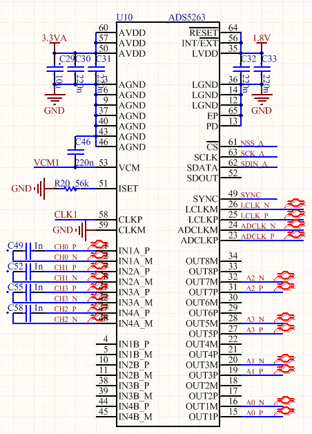
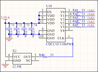
CLKP is a single ended 12.5M 3.3V CMOS clock.

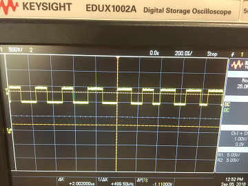
When I debugged the board, I found the ADCLK and LCLK is not related to CLKP.

The ADCLK and LCLK have the same output as I remove R45 and keep the CLKP Pin floating.

It seems the PLL in ADS5263 is not locked and behave like there is no CLKP input.

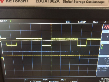
 CLKP wave: 12.5MHz, 3.3V CMOS

ADCLKP: about 300Hz clock, duty cycle is not stable

LCKP: about 4kHz, duty cycle is not stable

  • Hi Sheng,

    Welcome to TI E2E forum!

    Can you please clarify if the ADCLKP and LCKP waveforms that you have attached are with CLKP Pin floating (R45 removed)?
    Also can you provide the register configuration?
  • The waveforms that I attached are with CLKP Pin have 12.5MHz, 3.3V CMOS.
    I mean that weather or not CLKP Pin is floating, output of the ADCLKP and LCKP is the waveforms that attached.
    I am thinking the CLKM shouled not be connected to GND. A capacitor should be connected between CLKM and GND to keep CLKM biased.

    Here is my register configuration.
    ADDR DATA
    0 1
    0x38 0
    0x46 0x8800
    0x42 0x8020
  • Hi Sheng,

    How are you?

    Thank you for using our ADS5263 device.

    Could you please try the following methods

    on your own board schematic as below?

    Thank you!

    1) Please connect a capacitor (0.1uF) in series between your CLK1 signal (from your board) to CLKP (CLK+) clock pin.

    2) Please connect a capacitor (0.1uF) in series between your Ground signal (from your board) to CLKM (CLK-) clock pin.

    Thank you very much!

    Best regards,

    Chen