DLPC6401: Startup problems

Part Number: DLPC6401
Other Parts Discussed in Thread: SEGGER, DLPC350, DLP4501, DLP4500

Tool/software:

We’re having problems trying to boot the DLPC6401.  Several questions have come up while trying to troubleshoot the problem.

  • Where do I find a BSDL file for the DLPC6401?
  • What is the correct pull-down configuration on A21 and A22 for use with a 64Mbit flash?
  • Is the Macronix MX29LV640ETXEI-70G NOR flash supported by the DLPC6401?
  • What would prevent INIT_DONE from ever going high?
  • Where can I find v 2.0 of the DLPC6401 GUI?

Regarding (1), the datasheet says, “JTAG Boundary Scan Test Support”, but this requires the chain definition from a BSDL file.  We’ve successfully connected to the DLPC6401 via JTAG using a Segger J-Link and have been able to read the manufacturer & device ID with several programs (urjtag, openocd, TopJtag probe).  The manufacture & part ID read through JTAG match the DLPC350, but there are differences in the pinouts of the two parts, so I’m not sure if using the DLPC350’s BSDL is an option.

Regarding (2), the datasheet says, “the two most significant address bits (that is PM_ADDR_22 and PM_ADDR_21) are shared on pins GPIO_16 and GPIO_17 respectively”, and “if these GPIO pins are to be reconfigured as Program Memory Address pins, they require board-level pulldown resistors”.

Then there’s this table…

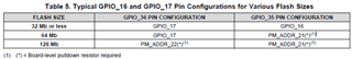
The reference design pulls down both PM_ADDR_21 and PM_ADDR_22.  Is the footnote just reaffirming that PM_ADDR_21 and PM_ADDR_22 are required to be pulled down, or does it indicate that GPIO_35 also needs to be pulled down for selection of the 64 Mbit part?  The reference design doesn’t help, as GPIO_35 and GPIO_36 are not connected to anything.

The datasheet says “until software reconfigures the pins from GPIO to Program Memory Address, upper portions of flash memory are not accessible”.  Is this handled by the bootloader? 

Regarding (3), in the post, “DLPC6401: Flash memory attached to the DLPC6401” by Alex Le in 2018, a response from Sanjeev says, “if the particular flash part is not supported by the controller then we cannot use it.”  The ref design uses a 32 Mbit NOR flash.  The schematic uses the Spansion/Cypress/Infineon S29JL032H and the BOM lists the S29GL032N90TFIR04, neither of which are still available.  We’ve selected the Macronix MX29LV640ETXEI-70G, a 64 Mbit NOR flash.  Will this part work?  Is there a list of parts somewhere that the controller supports?

The bootloader is the precompiled binary from the DPP6401_app_01.03.01_RVDS_3.1 archive we got from TI.  We had the flash preprogrammed with both the bootloader (DPP6401_APP_v1.3.1/dev/DPP6401/BootLoader/bootloader.bin) and the application (DPP6401_APP_v1.3.1/dev/app6401/app6401_data/flash_afe1000), but the device isn’t booting.  We suspect there may have been a problem with how the flash was programmed, so I attempted to use TI’s JTAGFlashProgrammer utility (DLPLCR4500JTAG_v1.0_WIN_2014_04_01.zip) to reprogram it.  We added an entry to the FlashDeviceParameters.txt file for the MX29LV640ET.  I tried to use the FTDI C232HM cable instead of the

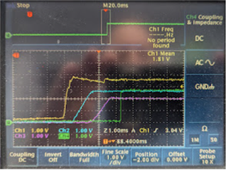
We never see INIT_DONE go high.  The voltage rails are all good prior to PWRGOOD going high, and POSENSE goes high after PWRGOOD.

Regarding (4), we’re primarily trying to determine if the processor is ever making it to the point to trying to read the flash, but it’s not clear what occurs within the controller prior to making INIT_DONE go high. 

Regarding (5), there’s an August 13th post from Sanjeev in response to Alex Le’s question on Flash memory attached to the DLPC6401 in which he says, “Put the working flash on the board, then use the DLPC6401 GUI version - 2 and experiment with flashing the part.”  We’ve only been able to find version 1 of the GUI.

  • Hello User,

    Welcome back to the E2E forums and we hope to assist you with your question. 

    Please give our team some further time to look into this issue. 

    Regards,

    Alex Chan

  • Hello User,

    Please see the following responses to your questions.

    For Question 1.) please see attached zip folder with JTAG BSDL file. 

    dpp6401_jtag_bsdl.zip

    For Question 2.)

    The table 5 is incorrect;y labelled and please ignore the GPIO 36 and GPIO 35. It should be GPIO 17 and GPIO 16. If you have a flash size of 64 Mb , you can use GPIO_17 freely but you cannot freely use GPIO_16 that pin must be used for PM_ADDR_21 and pulled down. 

    For Question 3.) 

    The basic requirements for the Flash part are listed in this word document. 

    Flash Memory Requirements.docx

    If any new part is use, the part info must be added into the FlashDeviceParameters.txt file. If the part info is not correct, then flash programming will not work.

    For question 4.)

    You can check the chip select and some of the address bits to see if they are toggling during initialization after powerup.

    For question 5.)

    I am not able to find a second version of the GUI at this time. 

    Regards,

    Alex Chan

  • Thanks Alex for providing the BSDL file and for the help so far.

    We've been able to successfully read, erase, & program the flash using the JTAGFlashProgrammer tool after adding an entry for the MX29LV640ET, so have confirmed that the bootloader is programmed into the part and that all of the parts had been correctly pre-programmed.  We expect that this demonstrates that the flash interface to the DLPC6401 is fine as well.  But, we still can't get the device to boot.  We never see the INIT_DONE pin go high, nor do we ever see the flash chip select change state, or the DMD_PWR_EN ever try to power the DMD.  Here's our power sequencing relative to the POSENSE signal...

    What's missing from the capture is the main SYS_PWR, 3.3V, that feeds the board, and the DLP core power (1.2V), which actually comes up first when PWR_EN is asserted.  The PG from 1V2 switches the 3V3 (yellow), and 3V3 is used to make 2V5 (blue) and 1V9 (not shown, but definitely comes up with 2V5), then 2V5 is used to make 1V8 (pink).  The PG from 1V8 flips POSENSE (green), and POSENSE is ANDed with the RESETn pin from a SYS_PWR monitor to create PWR_GOOD (not shown, but comes up at almost the exact same time as POSENSE.  

    Here's the 32MHz oscillator at the controller input...

    and finally, this is what the controller's oscillator input sees when POSENSE (yellow) goes high...

    What else should we be looking at?  Since we never see anything that would suggest the controller is trying to access the flash, I expect that some ROM boot loader command that's executed prior to trying to read from the flash is failing.  Is there a list somewhere of what checks are done prior to loading from flash, so we can have some idea of where to look for problems?  Thanks.

  • Hello Eric,

    Thanks for the further information, please give our team some time to look into this issue further. 

    Just to double check, has this system ever worked in the past or is this a new system that is being brought up for the first time?

    Regards,

    Alex Chan

  • Hi Alex,

    This is a new DLP system.  It's part of an existing product, but we're replacing an earlier TI DLP system due to parts obsolescence.  Thanks in advance for your help.

    Eric

  • Hello Eric,

    Thanks for the information so just to double check, does the application and bootloader work on the earlier TI DLP system and that older TI DLP system works and initializes fine?

    But now you have a new system with I assume an updated BOM but same schematic design but it now has this initialization error? Is your TI DLP system following this reference design https://www.ti.com/tool/TIDA-00782

    Regards,

    Alex Chan

  • Hi Alex,

    Yes, everything works on the earlier system.  It's been a medical product on the market for many years.  The earlier design and the new design both make use of the parallel video port, so we've confirmed compatibility of that interface with the similar DLPC350 by connecting the microcontroller & DSP components on the earlier design to the Panda board interface of the DLP LightCrafter 4500 (since both the DLPC350 and the DLPC6401 advertise compatibility with the DLP4500 DMD).  Yes, we've followed, as much as possible, the reference design to which you've linked.  We are using the DLP4500 though, and not the obsolete DLP4501.  I'd be glad to privately share our schematic if there's an option for you to review it.

  • Hello Eric,

    Thank you for the information. I will be passing off this thread to a coworker taking responsibility for this chipset. 

    Regards,

    Alex Chan

  • Eric,

    I or someone on my team will be taking this over.  I have some familiarity with the DLPC350, but not as much with the DLPC6401.

    I am sending you a friend invite so that you can share your schematic and possibly set up a phone meeting.

    Fizix

  • Eric,

    Please see my latest response in the friend chat.

    Fizix

  • Eric,

    Since we have moved this conversation offline, I would like to go ahead and close this thread.

    Fizix