Other Parts Discussed in Thread: DLPA200, , DLP7000
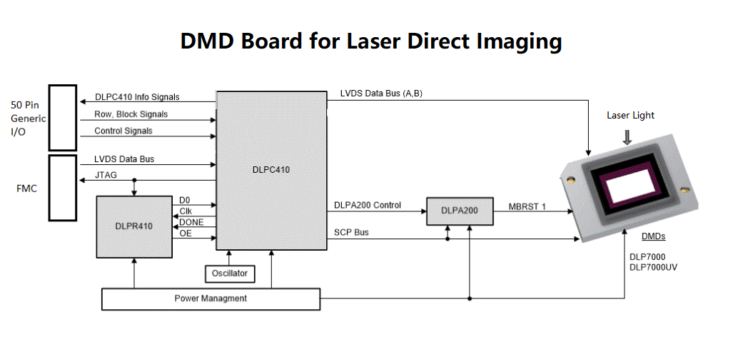
Based on the DLP Discovery 4100 Development Platform, I am putting the DLP7000 on the same PCB with DLPC410, minus the unused connections and components like one of the DLPA200 drivers, flex cable connectors and cables. I am also removing the application FPGA (V5), and adding corresponding LVDS signals (A[0:15], B[0:15], clock A&B, valid A&B) plus associated control signals and connectors as shown in the following functional block diagram:
I would like to know the following:
(1) Is this feasible?
(2) Since I am going to provide image data through the LVDS connections (assuming running at the same 400MHz double data rate from my own FPGA on a separate PCB), what is the "spec" for this interface?
(3) I could not find the 50MHz OSC for the DLPC410, only the one for the application FPGA, where is it?
More questions later ...


