Part Number: TCA6408A
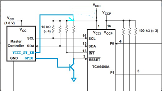
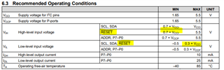
Customer needs to support a scenario where the Master I2C controller device goes into a standby or sleep state while the TCA6408A maintains the existing IO state on its GPIO pins. We believe this can be accomplished by making sure VccP is maintained above POR voltage and RESET voltage remains logic HI.
In addition, the customer also wants to minimize leakage paths in this condition. There is a concern that the I2C output of the Master device may not remain Hi-Z when in sleep/standby state and would lead to a current leakage path from the SDA/SCL pull-ups. One idea is to place a switch in the Vcci path to remove the power supply from both the TCA6408A and the I2C pull-up resistors as shown below:
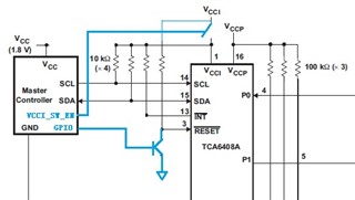
Is there any concerns about this idea? For example, the SDA/SCL inputs could be floating in this case which is usually not good for CMOS inputs. But since there is no Vcci, maybe the SDA/SCL input buffers not powered in this case so floating inputs would not matter?
An alternative idea is to add an I2C buffer/switch between the Master and TCA6408A to isolate the SDA/SCL interface when the Master goes to sleep/standby. This would add cost and power and is not preferred.