This thread has been locked.

If you have a related question, please click the "Ask a related question" button in the top right corner. The newly created question will be automatically linked to this question.

TPS65987D: I2C3 as master not working

Part Number: TPS65987D
Other Parts Discussed in Thread: BQ25703, TPS65987, TIDA-050047, BQ25792

I have made a test board with a TPS65987 to communicate to a BQ25703. I have read the SLVAE18 PDF and on table 1 it recommend to use I2C3 to connect the TPS65987 to chargers, etc.

My test board has the ability to jumper select which I2C port can be used to be master to:

the ports in blue go off to the I2C pins on an aardvark header.

When I use configure I2C3 as the master - no data on PD_SDA or clock PD_SCL

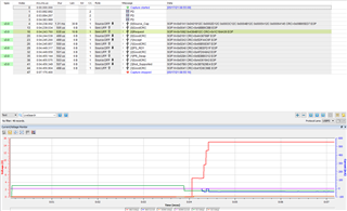
If I use I2C1 - I get data and clock. I verify this data using the battery management studio to read the registers on the BQ25703.

I check the GPIO setting for GPIO 5 & 6 and they are configured to be I2C pins.

Ideally I would need to use I2C1 to connect to an embedded controller (going forward from this design).

Can you please advise why I am unable to use I2C3 to communicate with the BQ25703 and why there's no data on it? Please find attached the project file that uses I2C3.

Test_DRP_5-5.pjt

  • Hi Chris,

    Are you testing in dead battery mode? Also, depending on what you need to control on the battery charger, you will have to input the I2C master event table and confirm the slave address is correct for the device. I will take a look at the project file and see if it's missing anything.

    Also, if you are looking for just PD + Charger, then you could also look into the TIDA-050047 which uses the TPS25750D and the BQ25792.

    Thank you,

    Hari

  • Hi Hari,

    thanks for offering to look at that file. Unfortunately I require alternative mode (display port) as well, other wise I would definitely be using it. I have continued on with my work using I2C1 port.

    I have another issue too. I have configured the event table to change the charge current of the charger with different power negotiations. However when I connect a USB-C power source to my board, there are no communications on the I2C bus telling the charger what current to use.

    The voltage on Vbus changes as per my configured contracts, and the PD controller does send data to the charger on attach and detach events, but it does not send data to configure the charge current.

    Could the negotiation have failed and thus this is the reason not charge current data is sent?

  • Hi Chris,

    The project file looks to be ok but I think maybe your schematic configuration of all of the I2C ports may be conflicting with each other sometimes. To confirm, you have jumpers but when you are testing the I2C3 port, you only have the jumpers connected for those pins and the other ones are disconnected, correct? I see that they are all tied together with only the jumpers separating them, however it looks like if I2C1 is connected, it has 2 labels the I2C1_SCL/SDA and also PD_SCL/SDA.

    I would recommend ideally separating all of the I2C ports and having their own dedicated resistors and pulling them up to LDO_3V3. What is the EEPROM connected to? Also I do not see the other block diagram to show the rest of the PD controller pins in the one you attached.

    If you see some I2C messages going through but not others, I suspect maybe some default settings on the charger could be preventing the PD controller to overwrite the charge current. I will try to see if someone from the charger team could help.

    If you are able to capture some scope shots of the I2C lines that would also help along with a PD log, which you could capture using a Total Phase PD Analyzer or similar.

    Thank you,

    Hari

  • Hi Hari,


    To confirm, you have jumpers but when you are testing the I2C3 port, you only have the jumpers connected for those pins and the other ones are disconnected, correct?

    Yes this is correct.

    What is the EEPROM connected to? Also I do not see the other block diagram to show the rest of the PD controller pins in the one you attached.

    Please see attached:

    I have removed R45, R43, C63, C61 and added 100k from the gate of Q8 to GND. However for my testing I am using the internal switches.

    as you can see the I2C1 pins are always connected to the Aardvark connector.

    If you are able to capture some scope shots of the I2C lines that would also help along with a PD log, which you could capture using a Total Phase PD Analyzer or similar.

    This is the PD data when the USB-C power supply I am using is connected (note I have change the voltage contract to negotiate 15V instead of 9V):

    The only I2C data I get is when only the I2C1 jumpers are shorted. Here is the data on POR (you should be able to see the data values hopefully):

    Here is some I2C data when a sink is attached (the sink is a ZY12PDN connected to a 10 ohms resistor) - so it can send data on a successful negotiation.

    Here is the CC data upon this sink device being attached:

    and here is the data when the USB-C supply is detached, telling the Bq25703 to return to OTG mode:

    I'd like to point out that the Instructions in SLVAE18 need updating to include a detach event to reset the BQ25703 to OTG mode, as I found when you detach your source and connect a sink, the sink does not receive any power. I added the event to the list and it worked, I was able to swap between sink and source devices.

  • Hi Chris,

    I will take a look at the data you provided, thank you. Also, are you saying that from this change to swap power role you were able to resolve your original issue? For the document you are referring to, yes we are in the process of updating it and it will be included in the next revision.

    Thank you,

    Hari

  • Also, are you saying that from this change to swap power role you were able to resolve your original issue?

    no, the original issue is still present.

    I would recommend ideally separating all of the I2C ports and having their own dedicated resistors and pulling them up to LDO_3V3.

    I have modified my design to have the pull -ups on each I2C port. Removing the links from jumpers 7, 8 & 9 I am able to now use the debug feature through the applications customisation tool.

    so I decided do some experimenting, and I have a development.

    I enabled I2C3 as master from the Global system Configuration(0x27) and configured the I2C master Configuration (0x64) so that the slave 1 Master Selection was I2C3.

    I then re-flashed the EEPROM, started the debug and looked at the I2C master config register:

    It still claims its using I2C1. So why has this happened?

  • Hi Chris,

    How did you Flash the EEPROM when you changed the configurations? Did you use the Flash from Current Project option on the GUI? Also, when you reflash, you will also need to power cycle the board to load the new configurations. 

    Also, do you happen to have the EVM?

    Thank you,

    Hari

  • How did you Flash the EEPROM when you changed the configurations? Did you use the Flash from Current Project option on the GUI? Also, when you reflash, you will also need to power cycle the board to load the new configurations. 

    I flashed it using the aardvark from total phase. I used the "flash from current project" option in the GUI. I disconnected all power from the board (USB-C, Battery connected to charger and the Aardvark itself) to power cycle and load the new config into the controller.

    Also, do you happen to have the EVM?

    No. I would have but after looking at it there was no easy/cheap way of interfacing it to the other device I wanted in my design to verify compatibility, so I made my board.

    Cheers,

    Chris

  • Hi Chris,

    I will try to discuss with my team to see what the issue could be and will provide you with some feedback next week. 

    In the meantime, I recommend double checking your schematic and comparing it to the TPS65987DEVM schematic which can be seen in the User's Guide for the EVM.

    Thank you,

    Hari

  • Hi Chris,

    I'm not sure what could be causing this behavior. Would you be able to verify that the PD is getting the new configurations from the flash instead of a default configuration or that the EEPROM is flashed correctly? Maybe in the project configurations, you could change the source capabilities and check if the PD log matches your changes after reflashing and power cycling.

    Another possibility could be maybe layout issues.

    Thank you,

    Hari 

  • Would you be able to verify that the PD is getting the new configurations from the flash instead of a default configuration or that the EEPROM is flashed correctly? Maybe in the project configurations, you could change the source capabilities and check if the PD log matches your changes after reflashing and power cycling.

    I can have a look, but am pretty confident that I have changed the source capabilities from 5V to 9V to 15V on separate occasions.

    I will export the project as a .bin file, upload to the flash, then use the aardvark to read the EEPROM using the total phase flash centre software an compare the bin file from the config tool and the flash centre using a bin comparison tool. I'll post my finding s soon.

  • Please find attached the file I exported from the application customisation tool and the one I extracted from the SPI-Flash after wards.BIN files for comparison.zip

    I have tried comparing the files but have been unable to glean anything from them, as I cannot find the information that maps the SPI-flash memory to the PD controllers.

  • Hi Chris,

    From looking at the 2 bin files, I think the EEPROM is not properly updating it's contents correctly. If you take a look at both files side by side, you will see at address 2000 that the data is not matching. Therefore, the Flash programming may be failing at some point since the EEPROM doesn't contain the same data.

    I think there may be an issue somewhere in the schematic or layout of your board causing some issues with the EEPROM. 

    Thank you,

    Hari

  • If you take a look at both files side by side, you will see at address 2000 that the data is not matching. Therefore, the Flash programming may be failing at some point since the EEPROM doesn't contain the same data.

    Thanks for taking a look at those files. This I did notice later on, but was not sure as to if I was interpreting the data correctly.

    I think there may be an issue somewhere in the schematic or layout of your board causing some issues with the EEPROM.

    I'm still confused as to how my layout could cause an address shift. surely if my layout would cause interference, it would interfere in all aspects of data, not just shifting the data to a different address? any advice you can offer in regards to this?

  • Hi Hari,

    I've had a logic analyser on my circuit and can confirm the data being sent to the EEPROM is correct and is in no way being altered by my layout. I've had 2 other engineers on this too and they have both concluded it is not my layout that would not cause an address shift.

    What I would like to know is what memory address the I2C3 port is enabled and what data should be present?

    I will also attempt to load my exported BIN file from the GUI to the board with the total phase flash tool. I will post my findings.

  • Hi Chris,

    It could be a Flash issue, another team member found that some EEPROMs are not compatible with the Aardvark adaptor. For the I2C3 address, for the PD controller it should just be 0x21 but I can double check. 

    I also noticed in register 0x62 you have set the Port 1 number and start index, could you also try moving from Port 1 index and number of indices to Common section?

    Thank you,

    Hari

  • I thought it was working for a second but turns out its not. I changed the index's like you said and the charger now charges but at the wrong current and I still cannot see data on the I2C3 port, so how this data is getting to the charger I have no idea.

    The port I2C1 is still being reported in uses from the debug mode. I have tried force writing the correct data to the register:

    I write 0x10000000000000000006b

    it reports successful write of 0x6b which is not correct. It seems I need that 1 bit at the beginning set and its just not setting it. Why is it not setting that 1 bit.

    Also from the raw view of this register is says that there should be 20 bytes, yet I count 21 and the interface technical manual states 16, I am really confused!

    I am starting to loose faith in this solution for our design.

  • Hi Chris,

    When you use the debug mode via I2C1, doesn't this mean that I2C3 also has jumpers connected in your design? Also, are you following the format shown in the datasheet for the I2C messages? If you are able to capture any type of I2C logs starting before the PD controller is turned on, I can take a look as it should send out those initial POR commands.

    Could you also post this question with the battery charger device in the title? This way the battery charger team could make sure that the data being sent is correct and to see if there might be another setting/register that might need to be configured before the current could be changed.

    Also which register are you referring to? The I2C master events Table will be different from the 0x64 register.

    Thank you,

    Hari 

  • When you use the debug mode via I2C1, doesn't this mean that I2C3 also has jumpers connected in your design?

    No. The jumpers are moved from one set to another.

    Also, are you following the format shown in the datasheet for the I2C messages?

    Surely this is handled by your software that I'm using via the Aardvark interface. Could you reference the section you are referring to?

    If you are able to capture any type of I2C logs starting before the PD controller is turned on, I can take a look as it should send out those initial POR commands.

    Will give it a look.

    Could you also post this question with the battery charger device in the title?

    How do I edit the title of this thread?

    Also which register are you referring to? The I2C master events Table will be different from the 0x64 register.

    0x64 register

  • For the I2C section, I am referring to Section 8.3.12.4 of the datasheet which contains some figures of the write/read protocol.

    When you get the I2C logs, I will take a look to see what is going on. 

    For the Title, I just meant to open a new e2e thread and have your charger part number in the title as that might be a separate question that the other team could help with.

    Thank you,

    Hari