This thread has been locked.

If you have a related question, please click the "Ask a related question" button in the top right corner. The newly created question will be automatically linked to this question.

SN65HVD255: What is the function and principle of Driver Dominant Time Out? Is it latch?

Part Number: SN65HVD255
Other Parts Discussed in Thread: ISO1042,

Hi team,

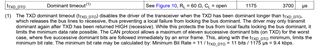
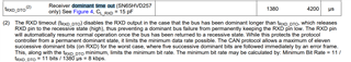
My customer is using SN65HVD255 for can transceiver and another node is ISO1042. Now, they found that after a few commands from MCU later, TXD no longer receive any commands anymore. I doubt that Driver Dominant Time Out would be root cause. Because customer is using ADM3051 for comparison, and ADI device will not have this issue. And I found that ADM3051 does not has this function.

So, could you help to explain the function and principle of Driver Dominant Time Out? Is it a latched function? How can we clear this fault?

  • Hi Miles,

    Here is a snippet from the datasheet:

    Essentially, when the bus has been held dominant for 1175 us - 3700 us a dominant time out will take place. As you explained this will disable the driver of the transceiver and then the bus will be released back to a recessive state. The way to check if a dominant time out is taking place is to measure the last dominant pulse, before the failure occurs, and see how long it lasted. If it was between 1175 us - 3700 us then it was most likely a dominant time out.

    To reset the driver the TXD pin must be returned back to high. As you can expect this will limit the data rate of this device. The calculation is shown in the data sheet and the minimum data rate is 9.4 kbps.

    The purpose of the dominant time out is to make sure there are no errors on your bus. If you are running at a rate above 9.4 kbps then if all of a sudden your bus is held dominant indefinitely the other CAN transceivers can no longer communicate on the bus. This could lead to some catastrophic safety problems in a vehicle or other systems. That is why dominant time out exists in the case that a device stops working at least the other CAN transceivers can continue to communicate.

    What is interesting about this device is that it also has a receiver DTO:

    The receiver (RXD) pin basically monitors the bus in normal mode, so if there is a dominant pulse for 1380us - 4200 us then the RXD output is disabled. The RXD output is enabled again once the bus is returned to a recessive state. Notice that the RXD DTO is longer than the TXD DTO. This means that a TXD DTO will automatically resolve an RXD DTO once the driver is disabled and the bus is returned back to recessive. If you calculated the minimum data rate based on the RXD DTO you would get 8 kpbs which is lower than the TXD DTO. This means that the actual minimum data rate is still 9.4 kbps.

    An RXD DTO would take place on the same device that causes a TXD DTO but it would also take place on any other device connected to the CAN bus that is transmitting the CAN bus data through it's RXD pin. However, as I already stated above the TXD DTO resolves the RXD DTO since it releases the bus to recessive automatically.

    If this answered your question don't forget to hit the button. If you have any more questions let me know.

    Best,

    Chris