A related question is a question created from another question. When the related question is created, it will be automatically linked to the original question.
If you have a related question, please click the "Ask a related question" button in the top right corner. The newly created question will be automatically linked to this question.
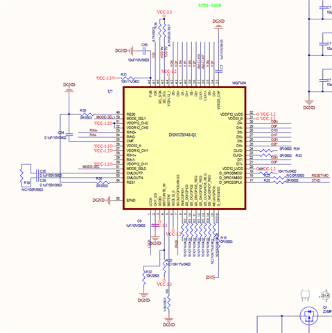
Yes, we would be happy to review the schematic. Could you share the full schematic that shows all the component connected to the UB948 device (e.g. power filters, RIN coupling caps ...)?
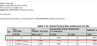
Re: "1. Could you explain the difference between OLDI and SWAP? Customer not sure which setting to choose."
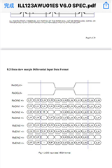
It’s just regarding data mapping differences. In the dual SWAP mode, the two series OLDI output are swapped as shown below:
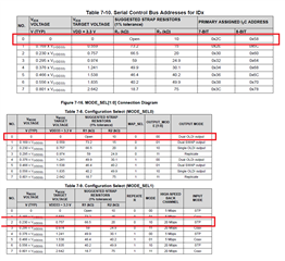
Re: "2. Could you explain the difference between STP and Coax? Customer not sure which setting to choose."
This is regarding what cable type you are using for the FPD link connection: Shielded Twisted Pair (STP) vs Coaxial cable (Coax).
Re: "3. Please explain the difference between "Repeater setting 0" and "Repeater setting 1"?"
This is regarding using the deserializer a repeater, which provides a mechanism to extend transmission over multiple links to multiple display devices. Please refer to the datasheet, section 7.3.14 Repeater, for more details.
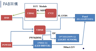
Re: "1.Please help confirm that the architecture is executable? "
Yes, UB941 should be able to link with UB948 as stated in the datasheet.
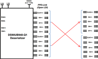
Re: "2. Is it possible to convert 4L-MIPI into 8L-LVDS according to the Block diagram(as Figure 1)? Currently Panel only accept 8L-LVDS !"
Yes, assuming that PCLK is within the allowed range, you can select dual OLDI output to achieve that as shown below:
When in a dual-link configuration, LVDS channels D0 to D3 carry ODD pixel data, and LVDS channels D4 to D7 carry EVEN pixel data. In this configuration the PCLK rate embedded within the 1-lane FPD-Link III frame can range from 50 MHz to 96 and CLK1 and CLK2 will operate at half the rate as PCLK. Please refer to the datasheet, section 7.4.1.2, for more details.
Re: "3. If 4L-MIPI can be converted to 8L-LVDS , will Image resolution become worse?"
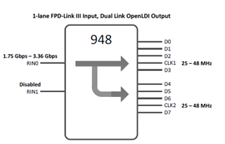
No, assuming that PCLK is within the allowed range, there should be no resolution issues. As explained above, LVDS channels D0 to D3 carry ODD pixel data, and LVDS channels D4 to D7 carry EVEN pixel data and CLK1 and CLK2 will operate at half the rate as PCLK.
Re: "4. If UB948 can send 8L-LVDS , Can UB948 output the sort of Figure 2 ?"
Yes, as explained above, this can be achieved by dual link OpenLDI output configuration. However, one thing I noticed from Figure 2 is that it looks like the display is expecting the data in SPWG bit mapping (MAPSEL = H). On the other hand, in the provided schematic, MODE_SEL0 was strapped for MAPSEL = L. So, there would be a mapping scheme conflict. So, you may need to fix the MODE_SEL0 strapping to select MAP_SEL = H, which changes the position of the MSBs and LSBs. Please refer to the datasheet, section 7.4.2 and 7.4.3, for more details.