This thread has been locked.

If you have a related question, please click the "Ask a related question" button in the top right corner. The newly created question will be automatically linked to this question.

TCAN1042V-Q1: VIH and VIL calculation questions

Part Number: TCAN1042V-Q1

 Hi My customer is using TCAN1042VDRQ1 and would like to ask some questions about parameters in datasheet:

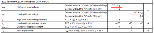
1. Can the parameters in the following specifications be understood as follows?

TXD, less than or equal to 0.3xVio, recognized as low, greater than or equal to 0.7xVio, recognized as high

RXD, less than or equal to 0.2xVio, recognized as low, greater than or equal to 0.8xVio, recognized as high


2. Why is there a difference in the recognition voltage between TXD and RXD?

Thank you.

  • Hi Zirui,

    The TXD terminal is an input to the device which requires the input signal to meet the listed thresholds to properly recognize the data. The RXD terminal is an output terminal and will drive an output signal with the specifications listed. The output characteristics are closer to logic-level references (Vio or GND) to account for possible losses between signal driver and receiver. This allows a device with similar input requirements to be compatible with these output characteristics even when driving a large load or through significant series resistance. 

    Let me know if this is clear and if you have any more questions.

    Regards,
    Eric Schott

  • Hi Scott

    Understand your first-half explanation. Due to the loss and "This allows a device with similar input requirements to be compatible with these output characteristics even when driving a large load or through significant series resistance." I am a little bit confused about: what does the loss come from and how to reduce it by setting output characteristics closer to logic-level? How to understand the compatible since I always need to use the device with proper input requirement in datasheet. Thank you.

  • Hi Zirui,

    Losses in digital signals can come from resistive loads such as biasing resistors or input impedances and complex impedances during switching like trace capacitance and via inductance. Having output signals closer to the logic levels (Vio and GND) helps to maintain proper input levels at a receiving device despite attenuation from these sources. 

    Regards,
    Eric Schott