This thread has been locked.

If you have a related question, please click the "Ask a related question" button in the top right corner. The newly created question will be automatically linked to this question.

DS90UB941AS-Q1: DSI Enable Disable Doesn't shows the Display even the video data available on DSI line

Part Number: DS90UB941AS-Q1
Other Parts Discussed in Thread: DS90UB928Q

Hi Team,

We are facing some issue with serializer configuration while getting the display.

Our Current HW configuration:

Qualcomm SOC (Android) --> MIPI --> Serializer (DS90UB941AS) --> FPD Link --> Deserializer (DS90UB928Q) --> LVDS Display.

Currently as a bringup process we are not configuring serializer in kernel rather we do it in userspace script. The configuration looks good, as we can see the display.

The problem we are facing today is we are not able to see the display soon after the script execution is done, rather we need to press android pwr key two times, which makes device to sleep and wakeup. (you can assume how android phone's pwr key we use to off and on the display).

I would like to understand this part why it has to goto off and On to get the display. Because as part of booting process I can see the dsi data is available. So I am epecting soon after the script executed I should see the available display., but its not happening.

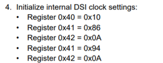
Below is my script. After executing this script ON and OFF makes the display up.

#! /system/bin/sh
i2cset -y 3 0x0c 0x01 0x08 b    #//Disable DSI

i2cset -y 3 0x0c 0x1E 0x01 b    #Select FPD-Link III Port 0
i2cset -y 3 0x0c 0x03 0x9A b    #Enable I2C_PASSTHROUGH, FPD-Link III Port 0


i2cset -y 3 0x0c 0x07 0x94 b    #Set Slave Address
i2cset -y 3 0x0c 0x08 0x94 b    #Set Slave Alias

i2cset -y 3 0x0c 0x1E 0x01 b    # Select FPD-Link III Port 0

i2cset -y 3 0x0c 0x40 0x05 b    # 001 : DSI/D-PHY Port 0 Digital Registers
i2cset -y 3 0x0c 0x41 0x21 b    # Select DSI_CONFIG_1 register  
i2cset -y 3 0x0c 0x42 0x60 b    # Set DSI_VS_POLARITY=DSI_HS_POLARITY=1

i2cset -y 3 0x0c 0x1E 0x01 b    # Select FPD-Link III Port 0                                                        
i2cset -y 3 0x0c 0x4F 0x8C b    # Set DSI_CONTINUOUS_CLOCK, 4 lanes, DSI Port 0

i2cset -y 3 0x0c 0x40 0x04 b    # Select DSI Port 0 digital registers
i2cset -y 3 0x0c 0x41 0x05 b    # Select DPHY_SKIP_TIMING register
i2cset -y 3 0x0c 0x42 0x02 b    # Write TSKIP_CNT value for 90 MHz DSI clock (800p, PCLK = 30 MHz)

i2cset -y 3 0x0c 0x01 0x00 b    #//Enable DSI

Can you please let us know what causes this issue? I want to understand more on DSI enable and disable part, to design the driver better.

  • Hello Jeshwanth,

    This sounds like it may be related to what is described in section 4.2 of this application note on DSI bringup: https://www.ti.com/lit/pdf/snla356 

    Please check that section for information on how to diagnose this potential implementation problem. Also please note that your initialization script should have several extra steps which are described in the power up init sequence section of the datasheet prior to the last line which enables DSI:

    Best Regards,

    Casey 

  • Hi Casey,

    Thanks for providing direction to debug this issue. From 4.2 section I use the resolution mentioned over there. Now display not coming at all, before atleast I use to see the display on Pwr key toggle two times, now nothing.

    Below is my last few lines of my device tree configuration for the panel I am using. In this bold lines I have added after section 4.2 resolution. Anything else u suspect in this configuration?

            qcom,mdss-dsi-on-command-state = "dsi_hs_mode";
            qcom,mdss-dsi-off-command-state = "dsi_hs_mode";
            qcom,mdss-dsi-h-sync-pulse = <1>;
            qcom,mdss-dsi-bllp-eof-power-mode;
            qcom,mdss-dsi-bllp-power-mode;
            qcom,mdss-dsi-traffic-mode = "burst_mode";
            qcom,mdss-dsi-lane-map = "lane_map_0123";
            qcom,mdss-dsi-lane-0-state;
            qcom,mdss-dsi-lane-1-state;
            qcom,mdss-dsi-lane-2-state;
            qcom,mdss-dsi-lane-3-state;
            qcom,mdss-dsi-panel-timings = [41 10 06 00 28 2c 0a 12 09 03 04 00];
            qcom,mdss-dsi-t-clk-post = <0x05>;
            qcom,mdss-dsi-t-clk-pre = <0x11>;
            qcom,mdss-dsi-bl-min-level = <1>;
            qcom,mdss-dsi-bl-max-level = <4095>;
            qcom,mdss-dsi-dma-trigger = "trigger_sw";
            qcom,mdss-dsi-mdp-trigger = "none";
            qcom,mdss-dsi-bl-pmic-control-type = "bl_ctrl_wled";
            qcom,mdss-dsi-reset-sequence = <1 20>, <0 2>, <1 20>;
            qcom,mdss-dsi-lp11-init;

  • One more thing I missed: I can see 0xbb (DSI_VC_DTYPE)

    i2cset -y 3 0x0c 0x40 0x04 b
    i2cset -y 3 0x0c 0x41 0x2A b
    i2cget -y 3 0x0c 0x42
    0xbb

  • Hello Jeshwanth,

    Please try 

    qcom,mdss-dsi-traffic-mode = "non_burst_sync_pulse";

    Best Regards,

    Casey 

  • Hi Casey,

    Tried "non_burst_sync_pulse" still the same. Any other information required from host side to analyse?

  • Hello Jeshwanth,

    I would recommend reaching out to Qualcomm for support on configuring the DSI driver here since we are not experts on that from the TI side. As for 941AS, your configuration looks correct for a basic configuration of PCLK from DSI clock mode where the source would be expected to be in non-burst sync pulse mode and to provide accurate DPI timing per the DSI standard. In terms of debugging the 941AS side specifically I would recommend to follow the flow chart provided in the app note I linked before as it gives a step by step process to narrow down on the problem area quickly and precisely. 

    Best regards,

    Casey