Part Number: SN65HVD24
Other Parts Discussed in Thread: THVD1450, SN65HVD22
Hi support team.
My customer uses the SN65HVD24 interconnected.
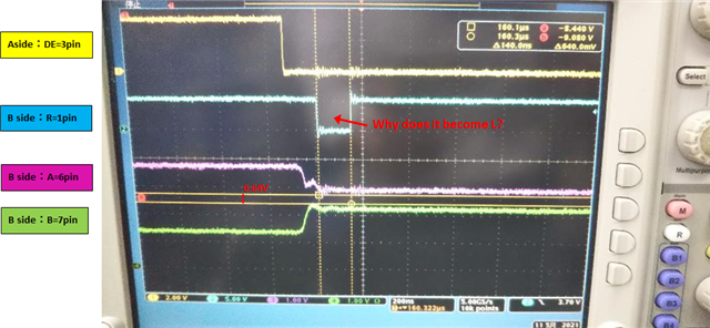
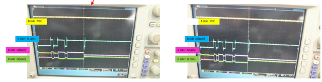
Distinguish the two SN65HVD24s from the A side and the B side.
In addition, there is an offset of about 0.6V on the B side because a resistor network circuit for failsafe is added.
My customer has designed the input on the B side to always be at the H level when the output on the A side is disabled, but that is not the case.
The waveform photograph below shows that the R output on the B side has reached the L level when the TX on the A side is disabled (DE = L).
Would you please give me some advice on what caused it?
Best regards,
HIga