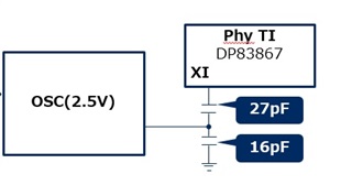
Our system is using DP83867IR with RGMII and it is able to link 1G with 5meter cable.
But it can not link with 100meter cable.
May I have a recommend some registers settings or Hard ware turning?
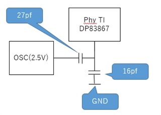
Our system is using DP83867IR with RGMII and it is able to link 1G with 5meter cable.
But it can not link with 100meter cable.
May I have a recommend some registers settings or Hard ware turning?