This thread has been locked.

If you have a related question, please click the "Ask a related question" button in the top right corner. The newly created question will be automatically linked to this question.

TMDS181: TMDS181 Technical Enquiry Questions

Part Number: TMDS181


Hi Team,

Customer designed TMDS181 and raised two questions. Would you please help?

1. About the termination of the setting in I2C mode, this register does not seem to be a fixed state. Would you please explain about this register usage?

2. Could you explain who writes 1 to the TMDS_CLOCK_RATIO_STATUS bit?
As datasheet the page 24, upon return to normal active operation from reasserted OE or reasserted HPD, the TMDS181 requires the source to write a 1 to the TMDS_CLOCK_RATIO_STATUS bit for the TMDS181 to resume 1/40th clock mode. The TMDS181 does not reset this bit based upon a DDC read transaction.

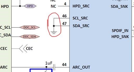
3. Can customer let the two pins of SCL_SRC and SDA_SRC be floating?

BR,

SHH

  • Hi, SHH

    1. For HDMI2.0 (greater than 3.4G data rate ), the TX_TERM_CTL must be set to 75-150ohm. HDMI1.4 allows two different terminations. For data rate less than 2G, you can set the termination to No Termination. For data rate between 2G and 3.4G, you can set the termination to No Termination or 150-300ohm for better signal integrity.

    2. As part of discovery, the source reads the sink’s E-EDID information to understand the capabilities of the sink. Part of this read is HDMI Forum Vendor Specific Data Block (HF-VSDB) MAX_TMDS_Character_Rate byte to determine the data rate supported. Depending upon the value, the source writes to the sink slave address 0xA8 offset 0x20 bit1, TMDS_CLOCK_RATIO_STATUS. The TMDS181 snoops this write to determine the TMDS clock ratio and thus sets its own TMDS_CLOCK_RATIO_STATUS bit accordingly.

    When the TMDS181 is put into a power-down state, the I 2C registers are cleared. This is important as the TMDS_CLOCK_RATIO_STATUS bit will be cleared. If cleared and HDMI2.0 resolutions are to be supported, the TMDS181 expects the source to write a 1 to this bit location. If this does not happen, the PLL will not be set properly and no video may be evident. In this particular case, you have to manually write to the DDC_TRAIN_SETDISABLE bit first to disable DDC training, and then write a '1' to the TMDS_CLOCK_RATIO_STATUS if HDMI2.0 resolutions are to be supported. 

    3. The SDA_SRC and SCL_SRC must be grounded. If not grounded, they would interpret system noise on these pins as signaling and hold up the DDC bus trying to send junk data.

    Thanks
    David