This thread has been locked.

If you have a related question, please click the "Ask a related question" button in the top right corner. The newly created question will be automatically linked to this question.

TPD1E10B06: ESD Testing ; +/- 15KV Air Discharge ; IEC 61000-4-2

Part Number: TPD1E10B06

We are using TVS diode, part no "TPD1E10B06DPYR" for ESD mitigation for medical device. We are following the IEC 60601-1-2 standard, sub clause IEC 61000-4-2. The maximum test voltage is +/-15KV (bipolar). We are passing +/- 8 KV test, but failing in +/- 12 & +/- 15 KV test (air discharge). The applicable test is air discharge, whenever the ESD probe was coming near conductor base sheet (below volume potentiometer) and near the thin wall of the switch (see fig. 1 below). I heard the discharge sound and the device used to stop function and then we had to manually re-start the device. 
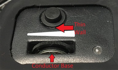
                                                  Fig. 1

Should we put TVS diode across conductor base plate and the ground and across the wire of the switch to the ground. Will the TVS diode work in this case, arrest the voltage.

Does two layer and four layer PCB layout will have any effect.

Pl suggest for the best possible outcome, for passing +/- 15KV ESD test (air).

Regards,

Tapas

  • Hi Tapas,

    Could you clarify what happens when test your system at 12 and 15 kV airgap? Is there damage to the system circuitry, or is normal operation just simply interrupted? 

    To answer your question about diode placement, yes. You should have an ESD on any exposed interface, including the button and the conductor base. Also, the shear number of layers on your PCB doesn't necessarily mean you will have better or worse ESD performance. It mainly depends on diode placement and grounding scheme. Please refer to our ESD Layout Guide for more details: https://www.ti.com/lit/an/slva680/slva680.pdf?ts=1626114776076&ref_url=https%253A%252F%252Fwww.google.com%252F 

    Regards,

    Matt Smith 

  • Dear Matt,

    During 12 KV airgap test, system was working fine. Output was nosiy, but within our acceptable limit. At 15 KV our device stopped responding  (there was no output). Later after restaring the device and waiting for 4 mins, it stated working. Later (after 4 hrs) we tested all the samples and they worked fine back in our office. They passed with criteria C (as per IEC standard), C criteria where user intervation is requied. Our is medical device, hence passing with criteria A is must to get all regulatory apporivals.  

    There was no damage to internal circuit, after inspecting the PCB. We had put TVS diode for USB line, now we will add for potentiometer metal part as well as for switch.

    We learn that TVS should be placed as close to the surge source ;  for switch, there is 3 cm wire coming from switch to the PCB, if we solder TVS in the PCB, then surge while travelling through wire can damge some parts as well. We are planning to put TVS next to switch, what is your take on this.

    Reagrds,

    Tapas

  • Hi Tapas,

    I think that's a good approach since it is an exposed interface that is unprotected. Be sure to read over that layout guide as well to minimize other ESD risks as well.

    Regards,

    Matt 

  • Dear Matt,

    We will do the changes and will test again. Thanks for your response.

    Regard,

    Tapas