This thread has been locked.

If you have a related question, please click the "Ask a related question" button in the top right corner. The newly created question will be automatically linked to this question.

TCAN4550: tcan4x5x: probe failed with error -22

Part Number: TCAN4550

Dear Team,

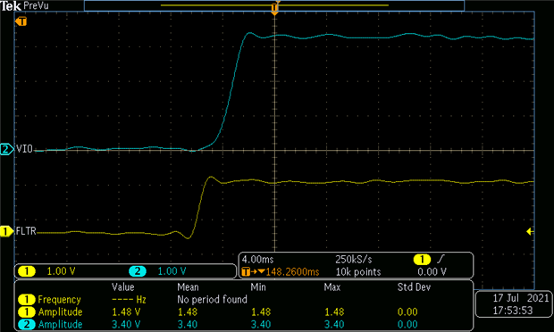
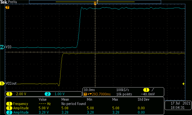
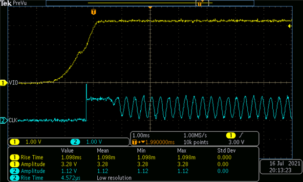
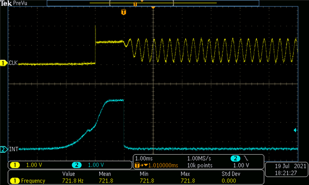
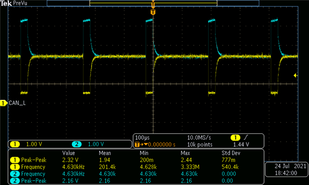
As I am using tcan4x5x driver in linux kernel version 4.14.98, I am facing the below issue

[ 27.788175] tcan4x5x spi0.0: Unsupported version number: 0
[ 28.034275] [<ffff0000087db7f0>] tcan4x5x_can_probe+0x318/0x550
[ 28.085188] [<ffff000009451ecc>] tcan4x5x_can_driver_init+0x18/0x20
[ 28.357443] [<ffff0000087db7f8>] tcan4x5x_can_probe+0x320/0x550
[ 28.408271] [<ffff000009451ecc>] tcan4x5x_can_driver_init+0x18/0x20
[ 28.681485] [<ffff0000087db804>] tcan4x5x_can_probe+0x32c/0x550
[ 28.732311] [<ffff000009451ecc>] tcan4x5x_can_driver_init+0x18/0x20
[ 29.004399] [<ffff0000087db80c>] tcan4x5x_can_probe+0x334/0x550
[ 29.055230] [<ffff000009451ecc>] tcan4x5x_can_driver_init+0x18/0x20
[ 29.088498] tcan4x5x spi0.0: Probe failed, err=-22
[ 29.097673] tcan4x5x: probe of spi0.0 failed with error -22

Please help me to solve this issue. I have traversed the previous queries, and made the changes accordingly, but the driver returns the value -22.

Best regards,

AyshaTT

  • Hi Aysha,

    Looking at this E2E post, it looks like error -22 may be associated with unsupported versions of the MCAN IP. Please make sure all your version definitions are accurate. I would read through this and related threads to see if this may be a similar issue. 

    As a disclaimer, I don't have much experience with the linux drivers for this device as they are open-source and primarily maintained by the linux community. We are most fit here to answer questions about the device and how it operates. 

    Regards,
    Eric Schott

  • Hi Eric,

    Our observation is that the tcan is not active after reset.

    We are doing reset as follows

    1. Reset GPIO is in low state when system boots up ( In DTS file Reset GPIO is configured as ACTIVE HIGH)
    2. Reset GPIO high for 60 microseconds 
    3. Keeping Reset GPIO low there after

    How we can make sure the TCAN device is up?

    Best regards,

    AyshaTT

  • Hi Aysha,

    When TCAN4550 initially powers on, is reset via the RST pin, or wakes from a sleep state, it will transition in to Standby mode. The easiest indication that the device is in this or any other active mode is the state of the INH pin. This is a battery-level open-source output meant to enable a local voltage regulator. It will be enabled whenever the device is not in its low-power sleep mode. To begin normal operation after a power-on, reset, or wake event, the device will need to be commanded to switch from Standby mode into Normal mode via a SPI write (Mode Control Register h0800, bits 7:6). 

    If INH does not assert (go to Vsup potential) after the reset command is sent, make sure that the device is properly supplied at Vsup. Keep in mind that because INH is an open-source output, it may take some time to fall to GND potential after it is de-asserted if no external leakage path to ground is present. 

    Regards,
    Eric Schott

  • Hi Eric,

    "To begin normal operation after a power-on, reset, or wake event, the device will need to be commanded to switch from Standby mode into Normal mode via a SPI write (Mode Control Register h0800, bits 7:6)."

    In tcan4x5x driver, the function  tcan4x5x_init(mcan_class) does the above operations. Under this function, it sets the register h0800.

    ret = regmap_update_bits(tcan4x5x->regmap, TCAN4X5X_CONFIG,
    TCAN4X5X_MODE_SEL_MASK, TCAN4X5X_MODE_NORMAL);

    Please let me know what other changes are to be done with respect to this in driver?

    Best regards,

    AyshaT

  • Hi Aysha,

    This looks correct and will change the device into normal mode as long as the SPI interface is responsive. Are you able to observe the INH output become asserted after the reset? Can you read back the value of the mode control bits in the config register to confirm the device is in normal mode? Are you still encountering the original error when you try to run the software?

    Regards,
    Eric Schott

  • Hi Eric,

    "This looks correct and will change the device into normal mode as long as the SPI interface is responsive"

    >> We are receiving SPI Mode value as 0. We had checked the SPI pins CS, CLK and MOSI are having expected observations. But MISO pin was having no changes it was in low state. This observation was done in oscilloscope. The configuration of these pins are proper.

    "Are you able to observe the INH output become asserted after the reset?"

    >> Yes

    "Can you read back the value of the mode control bits in the config register to confirm the device is in normal mode?"

    >> Since the MISO pin doesnot respond the value from the control bit is not able to read.

    "Are you still encountering the original error when you try to run the software?"

    >> Yes I am getting the same value as

    [ 29.088498] tcan4x5x spi0.0: Probe failed, err=-22
    [ 29.097673] tcan4x5x: probe of spi0.0 failed with error -22

    While checking Power Up Timing sequence in oscilloscope, we observed below

    1. VIO raises after FLTR and Vccout comes up. But in datasheet Figure 15. Power Up Timing, the FLTR and Vccout raises after VIO comes up. Whether this will leads to above issue? Since Vccout and FLTR are the output of the module, why both the voltages are coming before VIO voltage?
    2. Once CLK stabilizes, INT is not going high as provided in Power up Timing, Interrupt pin remains low for the initial 4 minutes. After 4 minutes INT is going high and VCCOUT and CLK is going low. Is this expected ? (We have provided a 10K pull-up for this INT pin)


       Below image shows the behavior of CLK and VIO,


    Whether all these observations are expected?

    Best regards,

    Aysha T

  • Hi Aysha,

    1. Vccout (and VFLT) are enabled while the device is in standby more. Typically, this is where the INH output would enable the 3.3V regulator so Vio can begin to be supplied. It is expected that Vccout come up soon after the device is powered on initially. Note figure 15 does not show a direct relationship between Vsup and Vio because Vio is supplied by an external source. The delay between Vsup becoming active and when Vccout becomes available is specified. 

    2. After initial power-up, the PWRON interrupt flag will be set, causing the nINT output to be asserted (pulled low). This status can only be accessed internally by the device once the clock signal is present. From the scope shots, it looks like the nINT signal does goe high for a short amount of time, but the pull-up resistor is too weak to raise the signal very high before the PWRON reset interrupt is recognized and the signal is driven low by TCAN4550. 
    After 4 minutes of inactivity in standby mode (not getting switched to normal mode), TCAN4550 will automatically go to sleep. While asleep, the INH output, Vccout, and clock amplifier are turned off. The nINT line will also go high-z. This is done to leave the device in the lowest-power state in the case that the local node did not start up correctly. To avoid this sleep state, the device must be put into normal mode via SPI write within tINACTIVE of initial startup or wake. 

    It sounds like the SPI registers are not responsive after startup. This leads me to believe that there may be a problem with the clock signal as this is required to access the internal SPI registers. 

    • Are the device diagnostic registers (h0000 - h000C) accessible via SPI? These registers do not require a clock input to be accessed. 
    • What is the source of the clock input to TCAN4550. Is this an crystal or a single-ended clock input? What is the desired clock frequency?
    • Please share a schematic if possible. I'm particularly interested in the crystal circuit if applicable. You can share this with me privately via email (see my E2E profile by clicking my name). 
    • Can you capture a long-term scope shot of the clock input? I would like to see if this signal cuts out at any point or becomes unstable. 

    Regards,
    Eric Schott

  • Hi Eric,

    Thanks for your detailed reply.

    Please find the replies for your question inline.

    "Note figure 15 does not show a direct relationship between Vsup and Vio because Vio is supplied by an external source.

    The delay between Vsup becoming active and when Vccout becomes available is specified"

    >> Can you please confirm that this observation of VIO voltage will not create any issue?

    "1.Are the device diagnostic registers (h0000 - h000C) accessible via SPI? These registers do not require a clock input to be accessed. "

    >> We are not able to read the values. The register values were returning zero.

    "2. What is the source of the clock input to TCAN4550. Is this an crystal or a single-ended clock input? What is the desired clock frequency?"

    >> It is a crystal. Clock frequency is 40MHz.

    "3. Please share a schematic if possible"

    >> We have shared schematic through mail.

    "4. Can you capture a long-term scope shot of the clock input?"

    >> Attached the clock capture.

    Note: Clock is stable and there is no cut till device goes to sleep mode (4 minutes duration).

    FYI,

    Currently interrupt is going high at the time of clock start up and goes low after 1milli second. Attached capture FYR.

    Looking forward for your reply.

    Best Regards,
    Aysha T

  • Hi Aysha,

    Thanks for the prompt reply and extra scope shots. The clock signal here looks good. Seeing this and hearing that the diagnostic registers are not responsive, I don't suspect that this is primarily a clock issue. That said, if possible I would recommend revising the crystal circuit to include a series resistor on the OSC1 (and OSC2) traces. This will allow for tuning of the circuit later on. 

    Can you capture scope shots of the SPI communication lines so we can confirm that format and electrical requirements are being met here? Please include MOSI, MISO, nCS, and SCLK. I would like to see a while SPI frame while still being able to distinguish the value of individual bits. If your scope has a logic analyser function, it would be good to include the decoded SPI info.

    Regards,
    Eric Schott

  • Hi Eric,

    Sorry for the delayed response.

    We observed the signals in SPI lines after commenting below lines of code,

    File: drivers/spi/spi-imx.c
    Function: static void spi_imx_buf_rx_swap_u32(struct spi_imx_data *spi_imx)
    Commented Line:  val &= spi_imx->word_mask;

    Function: static void spi_imx_buf_tx_swap_u32(struct spi_imx_data *spi_imx)
    Commented Line: val &= spi_imx->word_mask;

    We have tried below test cases for sending CAN,

    Test case 1: Board to board CAN test
        We are executing below commands,
        In Board-1:
               ip link set can0 up type can bitrate 125000
               candump can0

        In Board-2:
             ip link set can0 up type can bitrate 125000
             cansend can0 123#AABBCCDD

    Board-1 didnot print the value sent from Board-2. The CANH and CANL shows continuous data transfer. Attached the image of CANH(blue) and CANL(yellow) FYR.


    Test case 2: M_CAN Internal Loop Back Test Mode

    We set the register 16'h0800[21] = 1 and 16'h0800[0] = 1 for internal loopback. And executed below commands in a single board.
        
        ip link set can0 up type can bitrate 125000
        candump can0&
        cansend can0 123#AABBCCDD

    The value 123#AABBCCDD is not received in can0.
        

    Regards,
    Aysha T


  • Hi Aysha,

    Were you able to establish good SPI communications with the device? If so, how did you verify this? Are you able to consistently read and write (verified) information to/from the device? If not, please share the SPI captures so I can review the electrical and format data. 

    I am not too familiar with the Linux drivers that are not directly related to TCAN4550. If possible, let's keep this discussion high level: register values, desired configurations, electrical observations, etc. 
    During test 1, can you read the values of the interrupt registers while the device is transmitting these pulses? It looks like the device is sending error frames, though the pulses seem too short and infrequent for this data rate. I would like to see what the device is reporting. Furthermore, what are the characteristics of the CAN bus during this test? What is the termination value? How long are the cables? Are there any other passive components on the  CAN boards?

    For test case 2, "test mode" significantly changes the behavior of the device by disabling either the transceiver or CAN controller. In the case you describe (CAN Controller test mode), the transceiver is disable and the TXD and RXD functions are mapped to external pins GPO2 and GPIO1 respectively. This allows for the use of an external transceiver with the TCAN4550 CAN controller. During this mode, the CANH and CANL pins of the TCAN4550 are unused. 

    Regards,
    Eric Schott

  • Hi Eric,

    Thanks for the reply.

    Yes we are able to establish SPI communication. We verified with CRO and and also logic analyser. Yes we are able to read/write data to/from the device.

    During test 1, the interrupt value was high. Termination value i s 120ohm.  The cables is less than 1 meter.

    During test 2, we tested Figure 29. SPI and M_CAN Core Test Mode and Figure 30. M_CAN Internal Loop Back Test Mode. In Figure 29 test , there is no signal variations in GPIO and no prints received at candump. In Figure 30 test, the candump received the print sent from cansend.

    Best regards,
    Aysha T

  • Hi Aysha,

    Thanks for the extra information. This clears some things up for me. 

    During test 1, what is the value of the interrupt register ('h0820)? If an MCAN interrupt is indicated, please share the value of the MCAN interrupt register as well ('h0824). If a SPIERR is indicated, please share the value of the device status register ('h000C). 

    The CAN controller expects to see the values it drives on the TXD (GPO2) line shown back on the RXD (GPIO1) line. If it sees a different value appear here, it will either recognize it has lost arbitration (TXD=high, RXD=low) or that it is unable to drive the CAN bus (TXD=low, RXD=high). Either way, the device will not attempt to continue the CAN frame. During the Core test mode (Figure 29), are the GPIO1 and GPO2 pins connected together to externally loop back this signal?

    If the above case has been configured correctly, please read the interrupt register during both tests to see where the behavior diverges. Knowing the value of the interrupt register and corresponding other interrupts will help us identify why the device does not appear to transmit as expected. 

    Regards,
    Eric Schott

  • Hi Eric,

    During test 1, the value of 0x0820, 0x0824, 0x000C registers are captured in different positions,

    1. Before writing data "AABBCCDD" to fifo,

    • Interrupt register ('h0820 ) is 0.
    • MCAN interrupt register (h'0824) is 0.  
    • Device status register (h'000C) is 28000008 ( in hexadecimal).  

    2. After writing data "AABBCCDD" to fifo, A value is written into "Tx Buffer Add Request (h'10d0)".
    An interrupt happened and driver jumped to ISR service.In the interrupt service routine, the values are same as below

    • Interrupt register ('h0820 ) is 0.
    • MCAN interrupt register (h'0824) is 0.
    • Device status register (h'000C) is 28000008 ( in hexadecimal).

              Added additional information of Interrupt and Control register on interrupt,

    • Interrupt register (h'1050) is 1800 (in hexadecimal).
    • Control register (h'1018) is 8300 (in hexadecimal).

    "During the Core test mode (Figure 29), are the GPIO1 and GPO2 pins connected together to externally loop back this signal?"
    >> Yes, the GPIOs are connected together to support loopback.


    Best regards,
    Aysha T

  • Hi Aysha,

    It appears that the device is reporting an internal access error based on the status register values here. It's likely that this is causing the values read from the other interrupt register to be inaccurate. For example, I would expect the interrupt register to have some flag set when the external interrupt pin is asserted. 

    I'm looking into possible sources of this error and will get back to you by tomorrow. 

    Regards,
    Eric Schott

  • Hi Aysha,

    It looks like this internal access error can be the result of attempting to access an invalid address. Please ensure all address values are correct in the corresponding header file. 

    Is it possible to capture scope shots of the SPI communication between the MCU and TCAN4550? I would like to be able to see each bit in a frame to ensure that electrical and format requirements are met. This may also show us where a potentially invalid address appears during the initialization process. 

    In regards to the test mode tests you ran previously, please note that the "loopback mode" operates differently than "controller test mode" with the GPIOs connected. During the controller test mode, the RXD pin is not perceived as an incoming message as this would be the same as monitoring the bus state while driving an external transceiver. Therefore the device would not be any "prints received at candump" because the device is only transmitting, not receiving. This is likely why we see different results for the two test mode cases. 

    Regards,
    Eric Schott