Other Parts Discussed in Thread: SN65DSI84, , DSI-TUNER
Hello TI support team,
currently we are working on a new design where we integrated SN65DSI84-Q1 and have some issues with I2C configuration of SN65DSI84 adapting to our connected dual lvds panels.
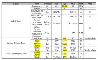
We use a 15.6'' dual lvds panel (resolution 1920 RGB x 1080) with following timing paramters you can see within this message attachements (Panel.jpg). Panel datasheet is also attached!
With the following I2C configuration of SN65DSI84 we get a valid test pattern on tft panel.
Our configured register values:
Reg=0x0a Value=0x85
==> HS_CLK_SRC=LVDS pixel clock derived from MIPI D-PHY channel A
==> LVDS_CLK_RANGE=010 – 62.5 MHz ≤ LVDS_CLK < 87.5 MHz
==> PLL_EN_STAT=1 – PLL enabled
Reg=0x0b Value=0x28 ==> DSI_CLK_DIVIDER=00101 – Divide by 6
Reg=0x0d Value=0x01 ==> PLL_EN=1 – PLL enabled
Reg=0x10 Value=0x26 ==> CHA_DSI_LANE=00 – Four lanes are enabled
Reg=0x12 Value=0x55 ==> CHA_DSI_CLK_RANGE=0x55 – 425 ≤ frequency < 430 MHz
Reg=0x18 Value=0x0c
==> CHB_24BPP_MODE=1 – Force 24bpp; LVDS channel B lane 4
==> CHA_24BPP_MODE=1 – Force 24bpp; LVDS channel A lane 4
==> LVDS_LINK_CFG=0 – LVDS Channel A and Channel B outputs enabled
==> VS_NEG_POLARITY=0 – VS is positive polarity driven
==> HS_NEG_POLARITY=0 – HS is positive polarity driven
==> DE_NEG_POLARITY=0 – DE is positive polarity driven
Reg=0x1a Value=0x00
==> CHB_LVDS_TERM=0 – 100Ω
==> CHA_LVDS_TERM=0 – 100Ω
Reg=0x20 Value=0xc0 (CHA_ACTIVE_LINE_LENGTH_LOW)
Reg=0x21 Value=0x03 (CHA_ACTIVE_LINE_LENGTH_HIGH) ==> 960 active pixel per line
Reg=0x24 Value=0x38 (CHA_VERTICAL_DISPLAY_SIZE_LOW)
Reg=0x25 Value=0x04 (CHA_VERTICAL_DISPLAY_SIZE_HIGH) ==> 1080 active lines for panel
Reg=0x28 Value=0x21 (CHA_SYNC_DELAY_LOW)
Reg=0x29 Value=0x00 (CHA_SYNC_DELAY_HIGH)
Reg=0x2c Value=0x23 (CHA_HSYNC_PULSE_WIDTH_LOW)
Reg=0x2d Value=0x00 (CHA_HSYNC_PULSE_WIDTH_HIGH)
Reg=0x30 Value=0x0a (CHA_VSYNC_PULSE_WIDTH_LOW)
Reg=0x31 Value=0x00 (CHA_VSYNC_PULSE_WIDTH_HIGH)
Reg=0x34 Value=0x23 (CHA_HORIZONTAL_BACK_PORCH)
Reg=0x36 Value=0x0a (CHA_VERTICAL_BACK_PORCH)
Reg=0x38 Value=0x23 (CHA_HORIZONTAL_FRONT_PORCH)
Reg=0x3a Value=0x0a (CHA_VERTICAL_FRONT_PORCH)
Reg=0x3C Value=0x10 (CHA_TEST_PATTERN) ==> Test pattern mode active!!!
==> Test pattern is OK on panel
==> set Reg=0x3C Value=0x00 (Test pattern mode inactive) only shows a black screen ==> data coming via MIPI-DSI input are not shown on panel
Our missunderstanding between register configuration and example configuration listed on page 34/35 of datasheet (www.ti.com/.../sn65dsi84.pdf
==> Example describes Horizontal active = 1920 or 0x780 but for us it's only working in test pattern mode if it is set to 1920/2=960 (0x3c0)
==> Example describes DSI_CLK_DIVIDER = 0010b – Divide by 6 but value 0010b is not Devider by 6 (reg=0x0b shows DSI_CLK_DIVIDER=00101 – Divide by 6)
Today we have also doublechecked register settings with TI "DSI-Tuner"-Tool and everything seems to be correctly set (see also attached DSI-Tuner input and output pages).
Can you please check what can be wrong in register config for our panel and how you can explain the missunderstanding within the data sheet example?
Thanks a lot for your support and your feedback as soon as possible.
Best Regards,
Johannes