This thread has been locked.

If you have a related question, please click the "Ask a related question" button in the top right corner. The newly created question will be automatically linked to this question.

SN65HVD72: SN65HVD72: Changing nRe pin, Rx out changes

Part Number: SN65HVD72

Hi Team,


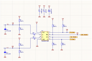
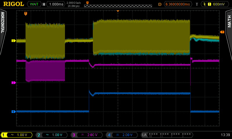
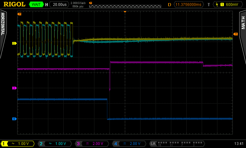
I use SN65HVD72 on one RS485 bus.

On one side of the bus (on the device)

when changing the nRE pin (from HIGHT to LOW and from LOW to HIGHT),

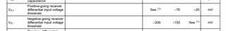
the Rx pin changes (LOW: duration 500ns)

It should be in a HIGHT state!


What's the problem?


Thanks and best regards,

Stjepan


  • Stjepan,

    Thanks for bringing this question to E2E! I've notified an expert of this thread and they will respond by Monday. We appreciate your patience on this.

    Regards,

    Eric Hackett 

  • Stjepan,

    Do you mean toggling REB (pin 2)? When REB=L, RX on, REB=H, RX off. When REB=L, what's the bus states (does R follow the bus)? When REB=H, what's the R (pin 1) load (does R stay H with a pull up resistor)? 

  • Hello ! 

    In my application I have to change the operation mode of the SN65HVD72DR from TX to RX and vice versa.

    The schematic of the SN65HVD72DR looks like this:

    The /RE and DE pins are controlled by my microcontroller (MCU).

    The MCU is powered at 2.5V. The SN65HVD72DR is powered at 3.3V.

    Here is the oscilloscope image with the problem:

    The osciloscope image displays the folowing:

    CH1 - B line of the SN65HVD72DR (Pin 7 of SN65HVD72DR)

    CH2 - A line of the SN65HVD72DR (Pin 6 of SN65HVD72DR)

    CH3 - R line of the SN65HVD72DR (Pin 1 of SN65HVD72DR)

    CH4 - /RE line of the SN65HVD72DR (Pin 2 of SN65HVD72DR)

    As you can see there is a glitch in CH3 (R line) on the right side of the image.

    The image does not disply the DE line (Pin 3 of SN65HVD72DR). DE line is changed from LOW to HIGH around the same time that I change /RE from HIGH to LOW. But DE and /RE are not toggled at the same time.

    This glitch is created when I change the /RE pin of the SN65HVD72DR from HIGH to LOW or vice versa.

    The zoomed glitch looks like this: 


    Does anyone have any suggestion why is this happening ?

    Thanks !

  • Thanks for the information to help me understand the issue. If you plot the differential bus voltage (A-B) on the scope, I think you will see this voltage is close to or below -200mV (SN65HVD72 receiver's threshold Vit-) for a short period of time, which makes the receiver generate a low (glitch). 

    Since DE and REB are controlled separately, you can delay the turn on time of REB to wait for bus voltage to settle. Another possible solution is to add termination resistors between A and B to help bus settling and also get better signal integrity.