This thread has been locked.

If you have a related question, please click the "Ask a related question" button in the top right corner. The newly created question will be automatically linked to this question.

DS90UB941AS-Q1: configure ds90ub941 as single DSI input and two FPD-LINK outputs

Part Number: DS90UB941AS-Q1

Hi Experts,

Our company is using DS90UB941 as display serializer. The connection is as below:
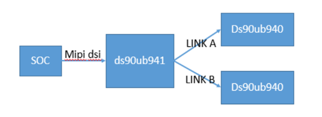
Now, it can display with single Link A or Link B. However, when I try to configure them to display together, replicate or splitter mode, some problems are encountered. Could you help to solve them?

Q1: ds90ub941 works at replicate mode

SOC outputs 720p60 MIPI DSI. After mipi dsi is valid, I need to set register 0x5B to 0x1(force single link mode), then reset it to 0x0(auto link mode).  Otherwise, both ds90ub940 cannot display images. But both ds90ub940s' lock and pass are active. If I set 0x5B to 0x1 and reset 0x5B to 0x0, both ds90ub940s can display successfully. 

Could you help to provide a simple register setting for replicate mode or modify my setting?

The following registers are ds90ub941's configuration.

/* disable dsi */
ds90ub941_write_reg(ds90ub941, addr, 0x01, 0x08);
/* Initialize internal DSI clock settings */
ds90ub941_write_reg(ds90ub941, addr, 0x40, 0x10);
ds90ub941_write_reg(ds90ub941, addr, 0x41, 0x86);
ds90ub941_write_reg(ds90ub941, addr, 0x42, 0x0A);
ds90ub941_write_reg(ds90ub941, addr, 0x41, 0x94);
ds90ub941_write_reg(ds90ub941, addr, 0x42, 0x0A);
/* enable continuous clock mode */
ds90ub941_write_reg(ds90ub941, addr, 0x4F, 0x80);
/* enable dsi reference clock mode */
ds90ub941_write_reg(ds90ub941, addr, 0x56, 0x00);
/* select DSI port0 */
ds90ub941_write_reg(ds90ub941, addr, 0x40, 0x04);
ds90ub941_write_reg(ds90ub941, addr, 0x41, 0x05);
ds90ub941_write_reg(ds90ub941, addr, 0x42, 0x12);
/* Enable DSI */
ds90ub941_write_reg(ds90ub941, addr, 0x01, 0x00);

Q2: ds90ub941 works at splitter mode

Another request is that we want to display two different videos on ds90ub941s.  

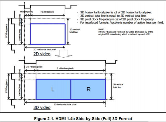
Figure 2-1 in doc SNLA308A says that 3D horizontal total pixel is x2 of 2D horizontal total pixel. If my 2D image horizontal total pixel is 1650(hbp 74, hsync 85, hfp 211, h_act 1280),  the 3D horizontal total pixel will be 1650x2=3300(hbp 148, hsync 170, hfp 422, h_act 2560). And vertical size doesn't change. Is it right?
Looking forward to your reply. Thank you very much.

Best regards,

Justin Ding

  • Hi Justin,

    Q1:

    This may be caused by an incorrect power-up sequence. Can you confirm your power-up sequence matches what is in the datasheet?

    Q2:

    That is correct, 3D horizontal total pixel = 2x2D horizontal pixel while 3D vertical total pixel = 2D vertical horizontal pixel

    Regards,

    Ben Dattilo

  • Hi Ben,

    Firstly, thanks for your information.

    Q1:

    Do you mean power up sequence in Section 10.2 in the datasheet? I have checked it. The difference is that my sequence initialize internal DSI clock immediately after disabling the DSI inputs. Does this matter?

    If the sequence must be matched, I have another question. Before soc MIPI DSI is available, I want to make I2C address mapping for remote deserializers and control their local GPIOs via I2C. Do you have any suggestions to implement it?

    Q2:

    Got it. I will make a 2x2D MIPI DSI on SOC and test it. Give feedback ASAP.

  • Hi Ben,

    Q1: After re-adjusting power-up sequence, dual FPD-LINKs could work well at replicate mode. Thanks~

    Q2: I encounter a problem when applying splitter mode. I configure the 2x2D horizontal pixels, but the displayer behind ds90ub940 is black. The registers configured for ds90ub941 is as below:

    # 2560x720@60 Symmetric Split Example - 2x 12800x720@60
    
    # Video 0 and Video 1 Parameters:
    # HACT = 1280
    # HFP = 214
    # HSYNC = 73
    # HBP = 83
    # VACT = 720
    # VFP = 19
    # VSYNC = 5
    # VBP = 6
    # PCLK = 74.25MHz 
    
    # DSI Superframe Dimensions:
    # HACT = 2560
    # HFP = 428
    # HSYNC = 146
    # HBP = 166
    # VACT = 720
    # VFP = 19
    # VSYNC = 5
    # VBP = 6
    # PCLK = 148.5MHz 
    
    # 4 Lanes DSI
    # DSI input port 0
    
    /* Disable DSI */
    ds90ub941_write_reg(ds90ub941, addr, 0x01, 0x08);
    /* enable continuous clock mode */
    ds90ub941_write_reg(ds90ub941, addr, 0x1E, 0x01);
    ds90ub941_write_reg(ds90ub941, addr, 0x4F, 0x8c);
    /* enable and dsi reference clock mode */
    ds90ub941_write_reg(ds90ub941, addr, 0x56, 0x00);
    /* configure TSKIP_CNT */
    ds90ub941_write_reg(ds90ub941, addr, 0x40, 0x04); // Select DSI Port 0 digital registers
    ds90ub941_write_reg(ds90ub941, addr, 0x41, 0x05); // Select DPHY_SKIP_TIMING register
    ds90ub941_write_reg(ds90ub941, addr, 0x42, 0x30); // Write TSKIP_CNT value for 148.5Mhz DSI clock frequency
    /* Enable Left/Right 3D processing */
    ds90ub941_write_reg(ds90ub941, addr, 0x5B, 0x07);
    ds90ub941_write_reg(ds90ub941, addr, 0x56, 0x80);
    /* Set line size */
    // Here is 1280 as default
    ds90ub941_write_reg(ds90ub941, addr, 0x32, 0x00);
    ds90ub941_write_reg(ds90ub941, addr, 0x33, 0x05);
    
    ds90ub941_write_reg(ds90ub941, addr, 0x1E, 0x1);
    /* set image size */
    ds90ub941_write_reg(ds90ub941, addr, 0x36, 0x00); // set crop start X(LSB)
    ds90ub941_write_reg(ds90ub941, addr, 0x37, 0x80); // set crop start X(MSB) and enable cropping
    ds90ub941_write_reg(ds90ub941, addr, 0x38, 0xFF); // set crop stop x(LSB) 1279
    ds90ub941_write_reg(ds90ub941, addr, 0x39, 0x04); // set crop stop x(MSB)
    ds90ub941_write_reg(ds90ub941, addr, 0x3A, 0x00); // set crop start y(LSB)
    ds90ub941_write_reg(ds90ub941, addr, 0x3B, 0x00); // set crop start y(MSB)
    ds90ub941_write_reg(ds90ub941, addr, 0x3C, 0xCF); // set crop stop y(LSB) 719
    ds90ub941_write_reg(ds90ub941, addr, 0x3D, 0x02); // set crop stop y(MSB)
    
    ds90ub941_write_reg(ds90ub941, addr, 0x1E, 0x2);
    /* set image size */
    ds90ub941_write_reg(ds90ub941, addr, 0x36, 0x00); // set crop start X(LSB)
    ds90ub941_write_reg(ds90ub941, addr, 0x37, 0x80); // set crop start X(MSB) and enable cropping
    ds90ub941_write_reg(ds90ub941, addr, 0x38, 0xFF); // set crop stop x(LSB) 1279
    ds90ub941_write_reg(ds90ub941, addr, 0x39, 0x04); // set crop stop x(MSB)
    ds90ub941_write_reg(ds90ub941, addr, 0x3A, 0x00); // set crop start y(LSB)
    ds90ub941_write_reg(ds90ub941, addr, 0x3B, 0x00); // set crop start y(MSB)
    ds90ub941_write_reg(ds90ub941, addr, 0x3C, 0xCF); // set crop stop y(LSB) 719
    ds90ub941_write_reg(ds90ub941, addr, 0x3D, 0x02); // set crop stop y(MSB)
    
    /* Initialize internal DSI clock settings */
    ds90ub941_write_reg(ds90ub941, addr, 0x40, 0x10);
    ds90ub941_write_reg(ds90ub941, addr, 0x41, 0x86);
    ds90ub941_write_reg(ds90ub941, addr, 0x42, 0x0A);
    ds90ub941_write_reg(ds90ub941, addr, 0x41, 0x94);
    ds90ub941_write_reg(ds90ub941, addr, 0x42, 0x0A);
    /* Enable DSI */
    ds90ub941_write_reg(ds90ub941, addr, 0x01, 0x00);

    Looking forward to your reply. 

    Best regards,

    Justin Ding

  • Hi Justin,

    I'm glad to hear the replicate mode is working well. As for the splitter mode:

    • Set the pattern generator to make sure the 940 is displaying correctly.
    • Try setting the IMG_DELAY control (registers 0x34 and 0x35) for each port. This is typically set to a small value (i.e. 12 clocks as per datasheet).

    Regards,

    Ben Dattilo

  • Hi  Ben,

    • For test pattern, do you mean that it works at splitter mode or just to verify whether 940 could display or not? 

    • I checked IMG_DELAY. Both of the dual ports are 0x0C( 12 clocks). If we need to modify them, is there any method to calculating them?

    Thanks~

    Regards,

    Justin Ding

  • Hi Justin,

    To clarify, try setting the pattern generator to test the lock between the SER and DEs, and verify the 940 is displaying what it should be with the pattern generator.

    Regards,

    Ben Dattilo

  • Hi Ben,

    I have a doubt that whether we need to check the lock between SER and DESs or not. Because they could work well with single link and replicate dual-link mode.

    Under splitter mode, the lock and pass both are active. For TP, do you have a working setting with 720p and 74.25Mhz pixel clock? If yes, can you share it to me? Thanks~

    Best regards,

    Justin Ding

  • Hi Justin,

    Thanks for the clarification. In this case it is likely not the lock between the SER and DES causing an issue. Can you provide a reg dump of the 941? Also, you can use the below script to read indirect CSI registers in the 940. This will show us the parameters of what is received by the DES.

    940CSIRead.txt
    board.WriteI2C(dev_addr, 0x6C, 0x0E)
    board.ReadI2C(dev_addr, 0x6D)
    
    board.WriteI2C(dev_addr, 0x6C, 0x0F)
    board.ReadI2C(dev_addr, 0x6D)
    
    board.WriteI2C(dev_addr, 0x6C, 0x10)
    board.ReadI2C(dev_addr, 0x6D)
    
    board.WriteI2C(dev_addr, 0x6C, 0x11)
    board.ReadI2C(dev_addr, 0x6D)
    
    board.WriteI2C(dev_addr, 0x6C, 0x12)
    board.ReadI2C(dev_addr, 0x6D)

    Regards,

    Ben Dattilo

  • Hi Ben,

    Here are the reg dumps of ds90ub941. Because I enable the secondary I2C address which is used for secondary port. So, I dump two parts. I2C address 0x0C is the default one, and 0x0D is the secondary one.

    # i2cdump -yf 0 0x0c
         0  1  2  3  4  5  6  7  8  9  a  b  c  d  e  f    0123456789abcdef
    00: 18 00 00 9a 00 00 58 58 e0 01 b7 de 47 30 00 00    ?..?..XX????G0..
    10: 00 99 00 8b 00 00 fe 1e 7f 7f 01 00 00 00 06 00    .?.?..?????...?.
    20: 0b 00 25 00 00 00 00 00 01 20 20 a0 00 00 a5 5a    ?.%.....?  ?..?Z
    30: 00 b9 00 05 0c 00 00 80 ff 04 00 00 cf 02 81 02    .?.??..?.?..????
    40: 10 94 00 00 00 00 00 00 00 00 00 00 00 00 00 8c    ??.............?
    50: 16 00 00 00 02 00 80 02 00 00 f9 07 07 06 44 4c    ?...?.??..????DL
    60: 22 02 00 00 10 00 00 00 00 00 00 00 00 00 20 00    "?..?......... .
    70: 00 00 00 00 00 00 00 00 00 00 00 00 00 00 80 00    ..............?.
    80: 00 00 00 00 00 00 00 00 00 00 00 00 00 00 00 00    ................
    90: 00 00 00 00 00 00 00 00 00 00 00 00 00 00 00 00    ................
    a0: 00 00 00 00 00 00 00 00 00 00 00 00 00 00 00 00    ................
    b0: 00 00 00 00 00 00 00 00 00 00 00 00 00 00 00 00    ................
    c0: 00 00 82 00 68 08 00 00 40 00 00 00 00 02 ff 00    ..?.h?..@....?..
    d0: 00 00 00 00 00 00 00 00 00 00 00 00 00 00 00 00    ................
    e0: 00 00 82 00 68 08 00 00 00 00 00 00 00 02 00 00    ..?.h?.......?..
    f0: 5f 55 42 39 34 31 00 00 00 00 00 00 00 00 00 00    _UB941..........
    # i2cdump -yf 0 0x0d
         0  1  2  3  4  5  6  7  8  9  a  b  c  d  e  f    0123456789abcdef
    00: 1a 00 00 9a 00 00 58 58 e2 01 0c 7e 47 30 00 00    ?..?..XX???~G0..
    10: 00 99 00 8b 00 00 fe 1e 7f 7f 01 00 00 00 06 00    .?.?..?????...?.
    20: 0b 00 25 00 00 00 00 00 01 20 20 a0 00 00 a5 5a    ?.%.....?  ?..?Z
    30: 00 b9 00 05 0c 00 00 80 ff 04 00 00 cf 02 81 02    .?.??..?.?..????
    40: 10 94 00 00 00 00 00 00 00 00 00 00 00 00 00 8c    ??.............?
    50: 16 00 00 00 02 00 80 02 00 00 f9 07 07 06 44 4c    ?...?.??..????DL
    60: 22 02 00 00 10 00 00 00 00 00 00 00 00 00 20 00    "?..?......... .
    70: 00 00 00 00 00 00 00 00 00 00 00 00 00 00 80 00    ..............?.
    80: 00 00 00 00 00 00 00 00 00 00 00 00 00 00 00 00    ................
    90: 00 00 00 00 00 00 00 00 00 00 00 00 00 00 00 00    ................
    a0: 00 00 00 00 00 00 00 00 00 00 00 00 00 00 00 00    ................
    b0: 00 00 00 00 00 00 00 00 00 00 00 00 00 00 00 00    ................
    c0: 00 00 82 00 78 00 00 44 40 00 00 00 00 02 ff 00    ..?.x..D@....?..
    d0: 00 00 00 00 00 00 00 00 00 00 00 00 00 00 00 00    ................
    e0: 00 00 82 00 68 08 00 00 00 00 00 00 00 02 00 00    ..?.h?.......?..
    f0: 5f 55 42 39 34 31 00 00 00 00 00 00 00 00 00 00    _UB941..........
    

    Also, the two DESs reg dumps are: (Address 0x70 is the DES on DOUT0, while address 0x71 is on DOUT1). May I ask what the reg's meaning? I re-read datasheet and don't find theirs description.

    # i2ctransfer -yf 0 w2@0x70  0x6C 0x0E
    # i2ctransfer -yf 0 w1@0x70 0x6D r1
    0x00
    # i2ctransfer -yf 0 w2@0x70  0x6C 0x0F
    # i2ctransfer -yf 0 w1@0x70 0x6D r1
    0x45
    # i2ctransfer -yf 0 w2@0x70  0x6C 0x10
    # i2ctransfer -yf 0 w1@0x70 0x6D r1
    0xfb
    # i2ctransfer -yf 0 w2@0x70  0x6C 0x11
    # i2ctransfer -yf 0 w1@0x70 0x6D r1
    0xe1
    # i2ctransfer -yf 0 w2@0x70  0x6C 0x12
    # i2ctransfer -yf 0 w1@0x70 0x6D r1
    0x12
    # i2ctransfer -yf 0 w2@0x71  0x6C 0x0E
    # i2ctransfer -yf 0 w1@0x71 0x6D r1
    0x00
    # i2ctransfer -yf 0 w2@0x71  0x6C 0x0F
    # i2ctransfer -yf 0 w1@0x71 0x6D r1
    0x45
    # i2ctransfer -yf 0 w2@0x71  0x6C 0x10
    # i2ctransfer -yf 0 w1@0x71 0x6D r1
    0xfb
    # i2ctransfer -yf 0 w2@0x71  0x6C 0x11
    # i2ctransfer -yf 0 w1@0x71 0x6D r1
    0xe1
    # i2ctransfer -yf 0 w2@0x71  0x6C 0x12
    # i2ctransfer -yf 0 w1@0x71 0x6D r1
    0x12
    

    Best regards,

    Justin Ding

  • Hi Justin,

    There appears to be a DSI error. Can you read the indirect register DSI_STATUS (Offset = 0x28)? The CSI registers you read are as follows:

    0x0E - Measured line length [7:0]

    0x0F - [FPS 30][FPS 60][FPS 240][Measured line length 11:8]

    0x10 - Measured frame length [7:0]

    0x11 - Measured frame length [15:8]

    0x12 - Measured frame length [23:16]

    Regards,

    Ben

  • Hi Ben,

    The DSI error has been fixed. It’s caused by MIPI DSI source without EOTp. According to program guide, this error doesn't cause any visual impact to the display. After masking DSI_NO_EOTPKT, DSI error is clear.

    There's another important message that you need to know. I enable DS90UB941 test pattern under splitter mode. Clock and timing are both used from my MIPI DSI source. Displayers are OK. Test pattern uses the flowing setting:

    i2ctransfer -yf 0 w2@0x0c 0x65 0x1
    i2ctransfer -yf 0 w2@0x0c 0x64 0x1
    i2ctransfer -yf 0 w2@0x0d 0x65 0x1
    i2ctransfer -yf 0 w2@0x0d 0x64 0x1
    

    However, if disable test pattern, the displayer is black. It seems that my MIPI DSI with 2560x720 needs to be checked.

    Best regards,

    Justin Ding

  • Hi Justin,

    I have rearranged the script you provided to more closely match the example in the Splitter Mode Operations app note, incase there is an order of operations issue. Note that TSKIP_CNT DSI parameter needs to be programed.

    941Rearrange.txt
    /* Disable DSI */
    ds90ub941_write_reg(ds90ub941, addr, 0x01, 0x08);
    /* enable continuous clock mode */
    ds90ub941_write_reg(ds90ub941, addr, 0x1E, 0x01);
    ds90ub941_write_reg(ds90ub941, addr, 0x4F, 0x8c);
    /*Enable Left/Right 3D processing to allow superframe splitting*/
    ds90ub941_write_reg(ds90ub941, addr, 0x5B, 0x07);
    ds90ub941_write_reg(ds90ub941, addr, 0x56, 0x00);
    /* Set line size */
    // Here is 1280 as default
    ds90ub941_write_reg(ds90ub941, addr, 0x32, 0x00);
    ds90ub941_write_reg(ds90ub941, addr, 0x33, 0x05);
    
    /*Crop Port0 720p image*/
    ds90ub941_write_reg(ds90ub941, addr, 0x1E, 0x1);
    ds90ub941_write_reg(ds90ub941, addr, 0x36, 0x00); // set crop start X(LSB)
    ds90ub941_write_reg(ds90ub941, addr, 0x37, 0x80); // set crop start X(MSB) and enable cropping
    ds90ub941_write_reg(ds90ub941, addr, 0x38, 0xFF); // set crop stop x(LSB) 1279
    ds90ub941_write_reg(ds90ub941, addr, 0x39, 0x04); // set crop stop x(MSB)
    ds90ub941_write_reg(ds90ub941, addr, 0x3A, 0x00); // set crop start y(LSB)
    ds90ub941_write_reg(ds90ub941, addr, 0x3B, 0x00); // set crop start y(MSB)
    ds90ub941_write_reg(ds90ub941, addr, 0x3C, 0xCF); // set crop stop y(LSB) 719
    ds90ub941_write_reg(ds90ub941, addr, 0x3D, 0x02); // set crop stop y(MSB)
    
    /*Crop Port1 720p image*/
    ds90ub941_write_reg(ds90ub941, addr, 0x1E, 0x2);
    ds90ub941_write_reg(ds90ub941, addr, 0x36, 0x00); // set crop start X(LSB)
    ds90ub941_write_reg(ds90ub941, addr, 0x37, 0x80); // set crop start X(MSB) and enable cropping
    ds90ub941_write_reg(ds90ub941, addr, 0x38, 0xFF); // set crop stop x(LSB) 1279
    ds90ub941_write_reg(ds90ub941, addr, 0x39, 0x04); // set crop stop x(MSB)
    ds90ub941_write_reg(ds90ub941, addr, 0x3A, 0x00); // set crop start y(LSB)
    ds90ub941_write_reg(ds90ub941, addr, 0x3B, 0x00); // set crop start y(MSB)
    ds90ub941_write_reg(ds90ub941, addr, 0x3C, 0xCF); // set crop stop y(LSB) 719
    ds90ub941_write_reg(ds90ub941, addr, 0x3D, 0x02); // set crop stop y(MSB)
    
    /* Initialize internal DSI clock settings */
    ds90ub941_write_reg(ds90ub941, addr, 0x40, 0x10);
    ds90ub941_write_reg(ds90ub941, addr, 0x41, 0x86);
    ds90ub941_write_reg(ds90ub941, addr, 0x42, 0x0A);
    ds90ub941_write_reg(ds90ub941, addr, 0x41, 0x94);
    ds90ub941_write_reg(ds90ub941, addr, 0x42, 0x0A);
    
    /*Program TSKIP_CNT DSI parameter on DSI Port0*/
    
    
    /* Enable DSI */
    ds90ub941_write_reg(ds90ub941, addr, 0x01, 0x00);


    Regards,

    Ben Dattilo

  • Hi Ben,

    Thanks for your great help. Splitter mode can work now. The root cause is that my MIPI DSI signal doesn't work well with 2560x720.Joy After tuning, DS90UB941AS could work now.

    Thanks again for your recent help.

    Best regards,

    Justin Ding