This thread has been locked.

If you have a related question, please click the "Ask a related question" button in the top right corner. The newly created question will be automatically linked to this question.

DS90UB954-Q1: How to debug register for 954 and 953 to verify which section of the problem is (sensor, 953, 954)

Part Number: DS90UB954-Q1
Other Parts Discussed in Thread: DS90UB953-Q1

Hi Team,

There is a good new that we  DIN DS90UB954-Q1 & DS90UB953-Q1

There is currently a project of rear mirror, using 954 + 953 and then 2-channel camera input!
But the problem is when 2-channel input, the screen will freeze within 10 minutes!


1. I would like to ask if there is any debug register for 954 and 953 to verify which section of the problem is (sensor, 953, 954)

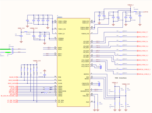
2. Please help check DS90UB954-Q1 SCH, THX

DS90UB954-Q1

  • Hi Kygo,

    Do you see a blank display? Or do you see a still image on the display? The way that our FPD-Link products work is that the Serializer sends video data to an RX port on a deserializer. The RX port has a FIFO line buffer, which stores a single line of video data before forwarding it out to the TX output port. The UB954 is not able to store an entire video frame, so it should not be causing frozen images to appear on screen. Your sensor might be sending a repeated image or your processor might be frozen.

    There are a number of registers that you can check on our devices. On the UB954, you can check registers 0x4D and 0x4E for error flags detected in the Rx ports. The status of the Tx port can be checked in register 0x35. If the TX_PORT_PASS bit is set, then it is outputting data out of its CSI-2 port. In the UB953, you can check register 0x52 for general status and lock. You can also check register 0x5D-0x60 for CSI errors from the sensor.

    And for your schematic, I will return with comments after the weekend.

    Best,

    Justin Phan 

  • Hi Kygo,

    Here are some comments on your schematic:

    1. The VDD11_FPD0, VDD11_FPD1, VDD11_CSI, and VDD11_D pins each need their own separate set of decoupling capacitors. Use a separate set of 4.7uF/0.01-0.1uF capacitors at each pin. Do not share capacitors across multiple pins.
    2. For the VDDIO pins, use a set of 1uF/0.1uF/0.01uF/0.01uF decoupling capacitors. The VDDIO pins can share this set of decoupling capacitors. Also, make sure to use a Ferrite Bead with Z = 120-Ohms @ 100MHz. The UB954 EVM uses MuRata BLM18SG121TN1D. Use the same or similar component.
    3. For the PDB pin, use a 33-kOhm pull-up resistor to VDDIO and a 10uF capacitor to GND. You used a 10-kOhm pull-up resistor instead.
    4. Remove the pull-up resistors at the PASS and LOCK pins. These are output pins that output a status.
    5. For GPIO3/INTB, use a 4.7-kOhm pull-up resistor to VDDIO if you would like to use the INTB functionality.
    6. For most applications, TI recommends a 4.7-kΩ pullup resistor to VDDIO at the SCL and SDA pins. But these resistor values can be adjusted based on data rate and capacitive load requirements. See the linked App Note for assistance in calculating new resistor values, if needed: https://www.ti.com/lit/an/slva689/slva689.pdf?ts=1627330437316&ref_url=https%253A%252F%252Fwww.google.com%252F
    7. For VDD18_P0 and VDD18_P1, use a shared set of 10uF/0.1uF/0.1-0.01uF decoupling capacitors. Also, make sure to use a Ferrite Bead with Z = 120-Ohms @ 100MHz to 1.8V.
    8. For VDD18_FPD0 and VDD18_FPD1, use a shared set of 10uF/0.1uF/0.1-0.01uF decoupling capacitors.
    9. For VDD18_CSI, use a set of 10uF/0.1uF/0.1-0.01uF decoupling capacitors.
    10. Add a 0.1uF capacitor to the IDX pin and the MODE pin.

    Best,

    Justin Phan

  • Justin

    Thank you so much for your help & feedback !

  • Hi Kygo,

    You are welcome. For now, I will close this thread. Feel free to post again if you have more questions or create a new post for a different topic.

    Best,

    Justin Phan