This thread has been locked.

If you have a related question, please click the "Ask a related question" button in the top right corner. The newly created question will be automatically linked to this question.

DS90UB954-Q1: Receiving Two DS90UB953-Q1 (1080p60) Video Stream

Part Number: DS90UB954-Q1

Hello, 

Below is the block diagram of my system.

I want to combine like both video stream and output to CSI-2 Port 0 in 4 data lanes and 1 clock lane. (assigning different virtual ID to both sensor)
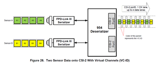
I used below Initialize sequence. but FPGA's MIPI CSI decoder is unable to detect proper MIPI signals.

// 0x60 DS954 Address
// 0x30 DS953 Address
// 0x6C Sensor Address

{0x60, 0x0C, 0x3F}, // Enable both RX0 & RX1
{0x60, 0x1F, 0x02}, // 800 Mbps

{0x60, 0x4C, 0x01}, // RX0
{0x60, 0x72, 0xE8},	// Sensor A VC0 to CSI-TX VC0 (CSI-2 input mode)
{0x60, 0x4C, 0x12}, // RX1
{0x60, 0x72, 0xED},	// Sensor B VC0 to CSI-TX VC1 (CSI-2 input mode)

{0x60, 0x33, 0x03}, // CSI EN & Cont Clock Enable

{0x60, 0x21, 0x01}, // Round Robin forwarding         

{0x60, 0x20, 0x00}, // forwarding all RX to CSI0

{0x60, 0x4C, 0x0F}, // RX0 sensor Read and Broadcast Write
{0x60, 0x58, 0x5E},
{0x60, 0x5C, 0x30},
{0x60, 0x5D, 0x6C},
{0x60, 0x65, 0x6C},
{0x30, 0x0B, 0x13},
{0x30, 0x0C, 0x26},
{0x30, 0x02, 0x53},
{0x30, 0x0E, 0x30},
{0x30, 0x0D, 0x03},
{0x30, 0x0D, 0x01},
{0x30, 0x0D, 0x03},

I am using both same sensor and resolution and frame rate are also same. So which forwarding method is best Round Robin or Basic Sync Forwarding?

is my initialization code is ok? Virtual ID assignment is OK?

What will be the data rate per lane of CSI-0 TX? (800Mbps)

  • Hi Ritesh,

    I am currently in the middle of reviewing your code. I will get back to you soon with comments. While I am doing so, could you confirm the following points?

    1. Are you able to detect LOCK and PASS? (Check register 0x4D in the UB954)
    2. Is the CSI TX Port outputting video data? (Check register 0x35 in the UB954)

    And for the forwarding mode, either Round Robin or Basic Sync can be used since you are using 2 identical image sensors. But synchronized forwarding has more stringent requirements. I recommend getting your system to work with Round Robin Mode first, before trying Basic Synchronized Forwarding Mode. 

    You can route up to 4 data lanes to a single Tx Port. If you plan on using Replication Mode, then you would route 2 data lanes to Tx Port 0 and 2 data lanes to Tx Port 1. The data rate of each lane is 800Mbps in this configuration. But it can be configured to be up to 1.6Gbps.

    Here are my comments so far:

    1. In lines 8-11, you are changing the way that VC-IDs are being remapped at each Rx Port. You do not necessarily need to include these lines, unless the VC-IDs of each video stream needs to be remapped. 
      1. By default, no remapping is done. Register 0x72 = 0xE4 (1110 0100). Two bits will be used to remap the incoming video stream's VC-ID. If the VC-ID of the incoming video stream at your selected Rx Port is 0, then bits 0x72[1:0] will be used to remap it to a new VC-ID between the possible values of 0 to 3. By default, it will be remapped to 0 (no change).
      2. If you set register 0x72 = 0xE8 (1110 1000), then a video stream that has a VC-ID of 1 will be remapped to a VC-ID of 2.
      3. The code example in the datasheet may not fit your application.
      4. What is the VC-ID of the video streams coming from your sensors? Some remapping may need to be done in order to make sure each video stream has a unique VC-ID.

    I will return with more comments soon.

    Best,

    Justin Phan 

  • Hi Ritesh,

    Here are additional comments:

    1. On line 19, you are setting register 0x4C = 0x0F (0000 1111). You are setting some RESERVED bits, which we do not recommend to do. If you would like to broadcast write to Rx Port 0 and Rx Port 1 registers, then I recommend setting register 0x4C = 0x03 (0000 0011).
      1. In register bit 0x4C[4], you are selecting an Rx Port to read the paged register settings. You can only select one Rx Port at a time. This setting does not matter, unless you want to read the paged register settings that you've made for one specific Rx Port.
    2. On line 21, you are setting the Serializer Alias. You should not do this under a broadcast write, since the alias should be unique. But if you would like to always send the same I2C messages to both serializers at the same time, then you can keep this setting.
      1. Registers 0x5B and 0x5C are automatically loaded from the connected serializer.
        1. For example, if the connected serializer at Rx Port 0 has an I2C address of 0x30 and you've set register bit 0x4C[4] = 0, then register 0x5B = 0x30 and register 0x5C = 0x18.
      2. You should not change register 0x5B, since that will cause your deserializer to be unable to find your connected serializer. But you may need to change register 0x5C, in order to ensure that the serializer aliases stored on the deserializer are all unique.
      3. Here is an example of setting unique Serializer Aliases:
        1. board.WriteI2C(0x60, 0x4C, 0x01) # Write to Rx Port 0 registers
          board.WriteI2C(0x60 ,0x58, 0x5E) # Enable pass through / 50Mbps BCC
          board.WriteI2C(0x60, 0x5C, 0x10) # Set the alias of serializer on Port 0 to 0x10 (any unique value)
        2. board.WriteI2C(0x60, 0x4C, 0x02) # Write to Rx Port 1 registers
          board.WriteI2C(0x60 ,0x58, 0x5E) # Enable pass through / 50Mbps BCC
          board.WriteI2C(0x60, 0x5C, 0x12) # Set the alias of serializer on Port 1 to 0x12 (any unique value)
    3. On lines 22 and 23, you are setting SlaveID[0] and SlaveAlias[0] under a broadcast write. This means that if you write an I2C message to the address stored in SlaveAlias[0], then the remote devices connected to the serializers on Rx Port0 and Rx Port1 will receive the message. 
      1. If both image sensors have the same I2C address and you would always send the same I2C message to both of them, then this setting is fine. 
    4. On line 26, you've set register 0x02 = 0x53. This means that you've set register bits 0x02[5:4] = 01 and enabled 2-lane configuration for the CSI data lanes. In general, we recommend setting register bits 0x02[5:4] = 11, in order to enable all 4 data lanes for video data transfer.
    5. On lines 27 - 30, I am not quite sure what you are trying to achieve. But it should not interfere with normal operation.
      1. On line 27, you set register 0x0E = 0x30, which means that you've set GPIO0 and GPIO1 as outputs. I recommend setting register 0x0E = 0x3C. This sets the unused GPIO2 and GPIO3 as inputs and enables their internal pull-down resistors.
      2. On lines 28-30, you are making GPIO0 and GPIO1 output a HIGH or LOW signal, based on the local register settings in bits 0x0D[3:0].

    Please let me know if you would like further clarification.

    Best,

    Justin Phan

  • Hi Justin,

    Thanks for the Reply.

    • Are you able to detect LOCK and PASS? (Check register 0x4D in the UB954)
    • Is the CSI TX Port outputting video data? (Check register 0x35 in the UB954)

    For RX0, 0x4D : 0x03, 0x3D : 0x01

    For RX1, 0x4D : 0x43, 0x3D : 0x01

    I recommend getting your system to work with Round Robin Mode first,

    Yes I am using Round Robin Mode. I can see activity on all 4 lanes in oscilloscope. And My FPGA RX Decoder detects valid frame_valid but not getting valid line_valid.

    What is the VC-ID of the video streams coming from your sensors?

    i believe both ov2740 sensors will stream with VC-ID of 0.

    On line 19, you are setting register 0x4C = 0x0F (0000 1111). You are setting some RESERVED bits, which we do not recommend to do.

    I know but i took reference from datasheet.

    • board.WriteI2C(0x60, 0x4C, 0x01) # Write to Rx Port 0 registers
      board.WriteI2C(0x60 ,0x58, 0x5E) # Enable pass through / 50Mbps BCC
      board.WriteI2C(0x60, 0x5C, 0x10) # Set the alias of serializer on Port 0 to 0x10 (any unique value)
    • board.WriteI2C(0x60, 0x4C, 0x02) # Write to Rx Port 1 registers
      board.WriteI2C(0x60 ,0x58, 0x5E) # Enable pass through / 50Mbps BCC
      board.WriteI2C(0x60, 0x5C, 0x12) # Set the alias of serializer on Port 1 to 0x12 (any unique value)

    I will try this and test. But with my existing code, i can successfully write both sensor. and read back.

    If both image sensors have the same I2C address and you would always send the same I2C message to both of them, then this setting is fine.

    Yes both sensor has same I2C Address.

    On line 26, you've set register 0x02 = 0x53. This means that you've set register bits 0x02[5:4] = 01 and enabled 2-lane configuration for the CSI data lanes. In general, we recommend setting register bits 0x02[5:4] = 11, in order to enable all 4 data lanes for video data transfer.

    This particular register is of DS953. My sensor output 2 lanes data so i configured 2 lanes.

    In summary, i can say that i can successfully write and read both sensor. I am getting LOCK and Pass for both RX0 & RX1. I am getting MIPI activity in all 4 CSI-2 output lanes. But only issue is that MY FPGA is somehow not detecting valid line valid so not outputting data to process further.

  • Hi Ritesh,

    Since you are able to get LOCK and PASS, then that is one less thing to worry about. And since you are able to read/write to your sensors, then we can place focus on other parts of your code.

    Since both of your OV2740 sensors will stream with VC-ID of 0, then you can try configuring one of your Rx Ports to remap the VC-ID map value for a VC-ID of 0. For example, you can try the following code:

    {0x60, 0x4C, 0x01}, // RX0
    {0x60, 0x72, 0xE4}, // Default value, no remap
    {0x60, 0x4C, 0x12}, // RX1
    {0x60, 0x72, 0xE5}, // Remap incoming VC-ID of 0 at Rx Port1 to a VC-ID of 1

    And could you also check to see if the expected video data is being sent to the Rx Ports on your UB954?

    You can do this by first selecting one of your Rx Ports in register 0x4C and then reading registers 0x73 - 0x76. You can also map the Line Valid/Frame Valid signals from each Rx Port to GPIOs on the UB954 and then probe the GPIOs to verify the video timing is as expected. The Frame Valid signal will pulse at the video frame rate and the Line Valid signal will pulse at the video line rate. See Section 7.4.13.2 GPIO Output Pin Control in the UB954 datasheet for instructions on how to configure the GPIOs.

    Best,

    Justin Phan

  • Hi Justin,

    Sorry for the late reply.

    I tried below setting but the same result i am getting. Getting Frame Valid in FPGA but no Line valid and no data output and virtual_channel_id output always showing 0.

    {0x60, 0x4C, 0x01}, // RX0
    {0x60, 0x72, 0xE4}, // Default value, no remap
    {0x60, 0x4C, 0x12}, // RX1
    {0x60, 0x72, 0xE5}, // Remap incoming VC-ID of 0 at Rx Port1 to a VC-ID of 1

    Below is the read register value for both RX0 & RX1

    0x73 : 0x04

    0x74 : 0x40

    0x75 : 0x09

    0x76 : 0x6A

    So, Line Count = 1088 & Line Len = 2410

    You can also map the Line Valid/Frame Valid signals from each Rx Port to GPIOs on the UB954 and then probe the GPIOs to verify the video timing is as expected. The Frame Valid signal will pulse at the video frame rate and the Line Valid signal will pulse at the video line rate. See Section 7.4.13.2 GPIO Output Pin Control in the UB954 datasheet for instructions on how to configure the GPIOs.

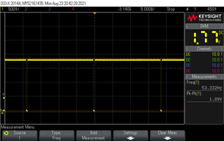
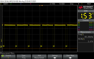
    I tried mapping Frame Valid & Line valid on GPIOs.

    Frame Valid waveform : 53.332 Hz

    Line Valid Waveform : 60 kHz

    are those value correct for 1080p60 2-camera multiplexed stream?

  • Hi Ritesh,

    Registers 0x73-0x74 report the line count for the most recently received video frame. Your reported line count is 0x0440 = 1088. Registers 0x75-0x76 report the line length in terms of bytes. Your reported line length is 0x096A = 2410. Since the sensors' data type is RAW10, then there are 10 bits per pixel. This means that 4 pixels are sent over 5 bytes. You can convert this to mean that (2410 bytes/line) * (4/5 pixels/byte) = 1928 pixels/line. 

    As a result, the detected line length and line count is 1928x1088. This is close enough to the expected 1920x1080 resolution of your sensors and should show that the deserializer is properly receiving the sensor video data. The Frame Valid waveform is also close enough to the expected 60 FPS, so I do not believe there is an issue regarding the video data being outputted by the sensor.

    In that case, could you provide a register dump of the UB954 and show if there are any error flags raised in registers 0x4D and 0x4E? This would allow me to investigate other possible causes. 

    Also, your setup includes 2 cameras actively sending video data. Does your application work when only one camera is actively sending video data? 

    Best,

    Justin Phan