This thread has been locked.

If you have a related question, please click the "Ask a related question" button in the top right corner. The newly created question will be automatically linked to this question.

DS90UB941AS-Q1: Setup ds90ub941 as single DSI input and two FPD-LINK outputs to two display

Part Number: DS90UB941AS-Q1

Hi Experts,

Our project is using a DS90UB941 via two ds90ub948 splitting two displays as below
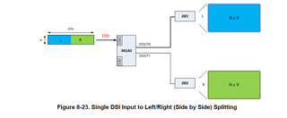
We follow snla308a.pdf set up DS90ub941 but both panel can't normal display anything.

Below are summary and some information about Setting

  1. Both of panel can't show anything,
  2. Dout0 we can access DeSerializer but Dout1 can't access DeSerializer by i2c.
  3. Could you help us checking do we have others setting have lose make both of panel can't normal display screen and Dout1 also can't access bt i2c? 

Input/Out video data

# 2560x800@60 Symmetric Split Example - 2x 12800x800@60

# Video 0 and Video 1 Parameters:
# HACT = 1280
# HFP = 60
# HSYNC = 28
# HBP = 40
# VACT = 800
# VFP = 8
# VSYNC = 3
# VBP = 5
# PCLK = 68935680 

# DSI Dimensions:
# HACT = 2560
# HFP = 120
# HSYNC = 56
# HBP = 80
# VACT = 800
# VFP = 8
# VSYNC = 3
# VBP = 5
# PCLK = 137871360

timings.width = 1280*2U;
timings.height = 800U;
timings.hFrontPorch = 60*2U;
timings.hBackPorch = 40*2U;
timings.hSyncLen = 28*2U;
timings.vFrontPorch = 8U;
timings.vBackPorch = 5U;
timings.vSyncLen = 3U;
timings.pixelClock = 68935680*2ULL

  • ds90ub941 setting

 /* ADDR    DAT */

    { 0x01, 0x08},
    { 0x1E, 0x01},
    { 0x03, 0x9A},
    /* Enable Left/Right 3D processing */
    { 0x5B, 0x07},
    { 0x56, 0x80},
    /* Here is 1280 as defaul*/
    { 0x32, 0x00},
    { 0x33, 0x05},
	/*Set up INTB*/
    { 0xc6, 0x21},

/*Crop Port0 1280X800 image*/
    { 0x1E, 0x01},
    { 0x36, 0x00},
    { 0x37, 0x80},
    { 0x38, 0xFF},
    { 0x39, 0x04},
    { 0x3A, 0x00},
    { 0x3B, 0x00},
    { 0x3C, 0x1F},
    { 0x3D, 0x03},

/*Crop Port1 1280X800 image*/
    { 0x1E, 0x02},
    { 0x36, 0x00},
    { 0x37, 0x80},
    { 0x38, 0xFF},
    { 0x39, 0x04},
    { 0x3A, 0x00},
    { 0x3B, 0x00},
    { 0x3C, 0x1F},
    { 0x3D, 0x03},

 /*Set DSI0 DSI_VS_POLARITY=DSI_HS_POLARITY=1*/
    { 0x1E, 0x01},
    { 0x40, 0x04},
    { 0x41, 0x21},
    { 0x42, 0x60},
    { 0x4F, 0x8C},

/*configure TSKIP_CN*/
    { 0x1E, 0x01},
    { 0x40, 0x04},
    { 0x41, 0x05},
    { 0x42, 0x2C},

 /*GPIO Setting*/
    { 0x0E, 0x33},
    { 0x0F, 0x03},
    { 0x10, 0x33},
 /*Enable DSI*/
    { 0x01, 0x00},

Ds90ub941 register dump

spm8666p1_64_bsp:/ # i2cdump -f -y 0 0xc
No size specified (using byte-data access)
     0  1  2  3  4  5  6  7  8  9  a  b  c  d  e  f    0123456789abcdef
00: 18 00 00 9a 00 00 58 00 00 01 12 00 67 30 33 03    ?..?..X..??.g03?
10: 33 00 00 ff 00 00 fe 1e 7f 7f 01 00 66 00 01 00    3.....?????.f.?.
20: 0b 00 25 00 00 00 00 00 01 20 20 a0 00 00 a5 5a    ?.%.....?  ?..?Z
30: 00 09 00 05 0c 00 00 80 ff 04 00 00 1f 03 81 02    .?.??..?.?..????
40: 04 05 2c 00 00 00 00 00 00 00 00 00 00 00 00 8c    ??.............?
50: 16 00 00 00 02 10 80 02 00 00 d9 07 07 06 44 46    ?...????..????DF
60: 22 02 00 00 10 00 00 00 00 00 00 00 00 00 20 00    "?..?......... .
70: 00 00 00 00 00 00 00 00 00 00 00 00 00 00 7e 00    ..............~.
80: 00 00 00 00 00 00 00 00 00 00 00 00 00 00 00 00    ................
90: 00 00 00 00 00 00 00 00 00 00 00 00 00 00 00 00    ................
a0: 00 00 00 00 00 00 00 00 00 00 00 00 00 00 00 00    ................
b0: 00 00 00 00 00 00 00 00 00 00 00 00 00 00 00 00    ................
c0: 00 00 82 00 78 00 21 44 40 00 00 00 00 02 ff 00    ..?.x.!D@....?..
d0: 00 00 00 00 00 00 00 00 00 00 00 00 00 00 00 00    ................
e0: 00 00 82 00 68 08 21 00 00 00 00 00 00 02 00 00    ..?.h?!......?..
f0: 5f 55 42 39 34 31 00 00 00 00 00 00 00 00 00 00    _UB941..........

Looking forward to your reply. Thank you very much.

Best regards,

Abbott Chung

  • Hi Abbot,

    In your script, please add the following lines of code before reenabling DSI as recommended in the datasheet to initialize DSI:

    board.WriteI2C(UB941AS,0x40,0x10) # Init DSI Clock Settings (From Section 10.2 of datasheet)
    board.WriteI2C(UB941AS,0x41,0x86) # Init DSI Clock Settings (From Section 10.2 of datasheet)
    board.WriteI2C(UB941AS,0x42,0x0A) # Init DSI Clock Settings (From Section 10.2 of datasheet)
    board.WriteI2C(UB941AS,0x41,0x94) # Init DSI Clock Settings (From Section 10.2 of datasheet)
    board.WriteI2C(UB941AS,0x42,0x0A) # Init DSI Clock Settings (From Section 10.2 of datasheet)

    Can you also read DSI_ERR_CFG_1 Register (0x23) from both port 0 and port 1 indirect registers?

    Regards,

    Ben Dattilo

  • Hi Ben.

    I have add the those setting at initial code, but still can't see the content at display.

    Below are dump from DSI_ERR_CFG_1 port0 & port1

    spm8666p1_64_bsp:/ # i2cset -f -y 0 0x0c 0x40 0x5
    spm8666p1_64_bsp:/ # i2cset -f -y 0 0x0c 0x41 0x23
    spm8666p1_64_bsp:/ # i2cget -f -y 0 0x0c 0x42
    0x7f
    spm8666p1_64_bsp:/ # i2cset -f -y 0 0x0c 0x40 0x9
    spm8666p1_64_bsp:/ # i2cset -f -y 0 0x0c 0x41 0x23
    spm8666p1_64_bsp:/ # i2cget -f -y 0 0x0c 0x42
    0x7f


    I also dump DSI port0 & port1 register information as below

    *********DSI0 REG*********
    0x01: 0x00
    0x02: 0x00
    0x03: 0x1d
    0x04: 0x14
    0x05: 0x2c
    0x06: 0x00
    0x07: 0x00
    0x08: 0x00
    0x0F: 0x3f
    0x10: 0x16
    0x11: 0x16
    0x12: 0x16
    0x13: 0x12
    0x14: 0x04
    0x15: 0x00
    0x20: 0x7f
    0x21: 0x60
    0x22: 0xff
    0x23: 0x7f
    0x28: 0x05
    0x29: 0xff
    0x2A: 0x3e
    0x2B: 0x8d
    0x2C: 0x06
    0x2D: 0x02
    0x30: 0x00
    0x31: 0x20
    0x32: 0x00
    0x33: 0x04
    0x34: 0x00
    0x35: 0x20
    0x36: 0x00
    0x37: 0x00
    0x38: 0x00
    0x3A: 0x02
    0x3B: 0x03
    *********DSI1 REG*********
    0x01: 0x00
    0x02: 0x00
    0x03: 0x1d
    0x04: 0x14
    0x05: 0x3a
    0x06: 0x00
    0x07: 0x00
    0x08: 0x00
    0x0F: 0x10
    0x10: 0x00
    0x11: 0x00
    0x12: 0x00
    0x13: 0x00
    0x14: 0x00
    0x15: 0x00
    0x20: 0x7f
    0x21: 0x00
    0x22: 0xff
    0x23: 0x7f
    0x28: 0x00
    0x29: 0x00
    0x2A: 0x00
    0x2B: 0x00
    0x2C: 0x00
    0x2D: 0x00
    0x30: 0x00
    0x31: 0x20
    0x32: 0x00
    0x33: 0x04
    0x34: 0x00
    0x35: 0x20
    0x36: 0x00
    0x37: 0x00
    0x38: 0x00
    0x3A: 0x02
    0x3B: 0x03

    Could you help checking the dsi need to modify or other need to change?

    Best regards,

    Abbott Chung

  • Hi Abbott,

    I've created a new script with your configuration. It appears port 1 is not configured correctly in your original script, based on what is seen in the DSI registers. Try running this and see if the issue is corrected.

    Superframe_Crop_2560x800.txt
    																																									
    board.WriteI2C(UB941AS,0x01,0x08)		#Disable DSI
    
    #Set HV polarity													
    board.WriteI2C(UB941AS, 0x1E, 0x01) 		#Select FPD-Link III Port 0
    board.WriteI2C(UB941AS, 0x40, 0x05)		#Select DSI Port 0 digital registers
    board.WriteI2C(UB941AS, 0x41, 0x21)		#Select DSI_CONFIG_1 register
    board.WriteI2C(UB941AS, 0x42, 0x60) 		#Set DSI_VS_POLARITY=DSI_HS_POLARITY=1
    board.WriteI2C(UB941AS, 0x1E, 0x02)		#Select FPD-Link III Port 1
    board.WriteI2C(UB941AS, 0x40, 0x09)		#Select DSI Port 1 digital registers
    board.WriteI2C(UB941AS, 0x41, 0x21)		#Select DSI_CONFIG_1 register
    board.WriteI2C(UB941AS, 0x42, 0x60) 		#Set DSI_VS_POLARITY=DSI_HS_POLARITY=1 
    															
    # set split mode, left/right 3D image, non-continuous clock mode															
    board.WriteI2C(UB941AS, 0x1E, 0x01)		#Select Port0													
    board.WriteI2C(UB941AS, 0x5B, 0x07)		#Force Splitter Mode													
    board.WriteI2C(UB941AS, 0x56, 0x80)		#Enable conversion of L/R image into alternating pixel image													
    board.WriteI2C(UB941AS, 0x4F, 0x8C)		#Set 4 lane DSI		
    											
    ##### Register 4F code configuration limited to use case of single DSI mode (RX Port 0) and no Altnerate line mode. If you would like to change the mode, please see register 0x4F [6:4]  in D/S															
    board.WriteI2C(UB941AS, 0x1E, 0x02)		#Select Port1													
    board.WriteI2C(UB941AS, 0x5B, 0x07)		#Force Splitter Mode													
    board.WriteI2C(UB941AS, 0x56, 0x80)		#Enable conversion of L/R image into alternating pixel image													
    board.WriteI2C(UB941AS, 0x4F, 0x8C)		#Set 4 lane DSI		
    											
    ##### Register 4F code configuration limited to use case of single DSI mode (RX Port 0) and no Altnerate line mode. If you would like to change the mode, please see register 0x4F [6:4] in D/S															
    															
    board.WriteI2C(UB941AS, 0x1E, 0x01)		# Select Port0													
    															
    board.WriteI2C(UB941AS, 0x32, 0x00)		#Set IMG_LINE_SIZE													
    board.WriteI2C(UB941AS, 0x33, 0x05)		#Set IMG_LINE_SIZE													
    board.WriteI2C(UB941AS, 0x36, 0x00)		#Set crop start X position (LSB)													
    board.WriteI2C(UB941AS, 0x37, 0x80)		#Set crop start X position (MSB)													
    board.WriteI2C(UB941AS, 0x38, 0xFF)		#Set crop stop X position (LSB)													
    board.WriteI2C(UB941AS, 0x39, 0x04)		#Set crop stop X position (MSB)													
    board.WriteI2C(UB941AS, 0x3A, 0x00)		#Set crop start Y position (LSB)													
    board.WriteI2C(UB941AS, 0x3B, 0x00)		#Set crop start Y position (MSB)													
    board.WriteI2C(UB941AS, 0x3C, 0x1F)		#Set crop stop Y position (MSB)													
    board.WriteI2C(UB941AS, 0x3D, 0x03)		#Set crop start Y position (LSB)													
    															
    board.WriteI2C(UB941AS, 0x1E, 0x02)		# Select Port1													
    															
    board.WriteI2C(UB941AS, 0x36, 0x00)		#Set crop start X position (LSB)													
    board.WriteI2C(UB941AS, 0x37, 0x80)		#Set crop start X position (MSB)													
    board.WriteI2C(UB941AS, 0x38, 0xFF)		#Set crop stop X position (LSB)													
    board.WriteI2C(UB941AS, 0x39, 0x04)		#Set crop stop X position (MSB)													
    board.WriteI2C(UB941AS, 0x3A, 0x00)		#Set crop start Y position (LSB)													
    board.WriteI2C(UB941AS, 0x3B, 0x00)		#Set crop start Y position (MSB)													
    board.WriteI2C(UB941AS, 0x3C, 0x1F)		#Set crop stop Y position (MSB)													
    board.WriteI2C(UB941AS, 0x3D, 0x03)		#Set crop start Y position (LSB)													
    															
    															
    board.WriteI2C(UB941AS, 0x1E, 0x01)		# Select Port0													
    board.WriteI2C(UB941AS, 0x40, 0x04)		# Select DSI digital page
    													
    board.WriteI2C(UB941AS, 0x41, 0x05)		# To reg 0x05 (TSKIP CNT)
    													
    board.WriteI2C(UB941AS, 0x42, 0x2C)		# Set value for DSI+CLK													
    board.WriteI2C(UB941AS, 0x40, 0x08)		# Select DSI digital page
    													
    board.WriteI2C(UB941AS, 0x41, 0x05)		# To reg 0x05 (TSKIP CNT)
    												
    board.WriteI2C(UB941AS, 0x42, 0x2C)		# Set value for DSI+CLK													
    															
    															
    board.WriteI2C(UB941AS, 0x01, 0x00)		#Enable DSI													
    

    Regards,

    Ben Dattilo

  • Hi Ben,

    After add those setting. I still can't see the screen on display.

    I have dump the latest register as below, could you help checking it.

    spm8666p1_64_bsp:/ # i2cdump -f -y 0 0xc
    No size specified (using byte-data access)
         0  1  2  3  4  5  6  7  8  9  a  b  c  d  e  f    0123456789abcdef
    00: 18 00 00 9a 00 00 58 00 00 01 13 00 67 30 33 03    ?..?..X..??.g03?
    10: 33 00 00 ff 00 00 fe 1e 7f 7f 01 00 6e 00 01 00    3.....?????.n.?.
    20: 0b 00 25 00 00 00 00 00 01 20 20 a0 00 00 a5 5a    ?.%.....?  ?..?Z
    30: 00 09 00 05 0c 00 00 80 ff 04 00 00 1f 03 81 02    .?.??..?.?..????
    40: 10 94 00 00 00 00 00 00 00 00 00 00 00 00 00 8c    ??.............?
    50: 16 00 00 00 02 10 80 02 00 00 d9 07 07 06 44 46    ?...????..????DF
    60: 22 02 00 00 10 00 00 00 00 00 00 00 00 00 20 00    "?..?......... .
    70: 00 00 00 00 00 00 00 00 00 00 00 00 00 00 7f 00    ..............?.
    80: 00 00 00 00 00 00 00 00 00 00 00 00 00 00 00 00    ................
    90: 00 00 00 00 00 00 00 00 00 00 00 00 00 00 00 00    ................
    a0: 00 00 00 00 00 00 00 00 00 00 00 00 00 00 00 00    ................
    b0: 00 00 00 00 00 00 00 00 00 00 00 00 00 00 00 00    ................
    c0: 00 00 82 00 78 00 21 44 40 00 00 00 00 02 ff 00    ..?.x.!D@....?..
    d0: 00 00 00 00 00 00 00 00 00 00 00 00 00 00 00 00    ................
    e0: 00 00 82 00 68 08 21 00 00 00 00 00 00 02 00 00    ..?.h?!......?..
    f0: 5f 55 42 39 34 31 00 00 00 00 00 00 00 00 00 00    _UB941..........

    DSI register dump

    *********DSI0 REG*********
    0x01: 0x00
    0x02: 0x00
    0x03: 0x1d
    0x04: 0x14
    0x05: 0x2c
    0x06: 0x00
    0x07: 0x00
    0x08: 0x00
    0x0F: 0x7f
    0x10: 0x06
    0x11: 0x06
    0x12: 0x06
    0x13: 0x18
    0x14: 0x04
    0x15: 0x08
    0x20: 0x7f
    0x21: 0x60
    0x22: 0xff
    0x23: 0x7f
    0x28: 0x01
    0x29: 0xff
    0x2A: 0x3e
    0x2B: 0x04
    0x2C: 0x07
    0x2D: 0x00
    0x30: 0x00
    0x31: 0x20
    0x32: 0x00
    0x33: 0x04
    0x34: 0x00
    0x35: 0x20
    0x36: 0x00
    0x37: 0x00
    0x38: 0x00
    0x3A: 0x02
    0x3B: 0x03
    *********DSI1 REG*********
    0x01: 0x00
    0x02: 0x00
    0x03: 0x1d
    0x04: 0x14
    0x05: 0x2c
    0x06: 0x00
    0x07: 0x00
    0x08: 0x00
    0x0F: 0x10
    0x10: 0x00
    0x11: 0x00
    0x12: 0x00
    0x13: 0x00
    0x14: 0x00
    0x15: 0x00
    0x20: 0x7f
    0x21: 0x60
    0x22: 0xff
    0x23: 0x7f
    0x28: 0x00
    0x29: 0x00
    0x2A: 0x00
    0x2B: 0x00
    0x2C: 0x00
    0x2D: 0x00
    0x30: 0x00
    0x31: 0x20
    0x32: 0x00
    0x33: 0x04
    0x34: 0x00
    0x35: 0x20
    0x36: 0x00
    0x37: 0x00
    0x38: 0x00
    0x3A: 0x02
    0x3B: 0x03
    

    Best regards,

    Abbott Chung

  • Hi Abbott,

    • In the 941 datasheet, there are two Power-Up and Initialization sequences described. Are you following Sequence A or Sequence B? Can you provide oscilloscope captures showing the initialization sequence of VDDx, PDB, DSI, PCLK?
    • Can you provide a reg dump of the 948 as well?
    • Your mode select shows the device is in coax mode. Are you using coax cables?

    Regards,

    Ben

  • Hi Ben,

    • After get power on sequence waveform, I will attach to E2E
    • Below is the DeSerializer register dump.

    spm8666p1_64_bsp:/ # i2cdump -f -y 0 0x2c
    No size specified (using byte-data access)
         0  1  2  3  4  5  6  7  8  9  a  b  c  d  e  f    0123456789abcdef
    00: 58 04 00 f0 fe 1e 00 18 00 00 00 00 00 00 00 00    X?.???.?........
    10: 00 00 00 00 00 00 00 00 00 01 00 00 03 15 55 05    .........?..??U?
    20: 99 00 40 20 08 00 83 84 01 00 00 00 00 00 00 00    ?.@ ?.???.......
    30: 00 00 90 25 01 00 00 8e 00 00 00 00 20 e0 23 00    ..?%?..?.... ?#.
    40: 43 03 03 00 60 88 00 00 0f e2 00 08 00 00 63 00    C??.`?..??.?..c.
    50: 03 10 00 01 80 00 00 00 00 7f 20 20 00 00 00 00    ??.??....?  ....
    60: 00 00 00 00 10 00 00 00 00 00 00 00 00 00 00 00    ....?...........
    70: 00 00 00 07 07 08 00 00 00 00 00 00 02 00 00 00    ...???......?...
    80: 00 00 00 00 00 00 00 00 00 00 00 00 00 00 00 00    ................
    90: 00 00 00 00 00 00 00 00 00 00 00 00 00 00 00 00    ................
    a0: 00 00 8c 00 00 00 00 00 00 00 00 00 00 00 00 00    ..?.............
    b0: 00 00 00 00 00 00 00 00 00 00 00 00 00 00 00 00    ................
    c0: 00 00 00 00 00 00 00 00 c0 00 00 00 00 00 00 00    ........?.......
    d0: 00 00 00 00 00 00 00 00 00 00 00 00 00 00 00 00    ................
    e0: 00 00 00 00 00 00 00 00 00 00 00 00 00 00 00 00    ................
    f0: 5f 55 42 39 34 38 00 00 00 00 00 00 00 00 00 00    _UB948..........


    • No, we are not use coax. we use STP

    Best regards,

    Abbott Chung

  • Hi Abbott,

    If you are using STP, you need to change the MODE_SEL1 on the 941, as it is currently set to coax mode. Table 8-10 in the datasheet shows the Strap Configuration for MODE_SEL1, and register 0x13 shows the status of MODE_SEL0 and MODE_SEL1. The 948 however appears to already be set to STP mode.

    Regards,

    Ben

  • Hi Ben,

    Our EE have checking the hardware setting. even change to STP mode it still can't see the content.

    reg  0x13  = 0xDF

    BR,

    Abbott

  • Hi Abbott,

    Have you verified what powerup/initialization sequence is being used? Also, try doing a soft reset towards the end of your script. To do this, write 0x01 to register 0x01. This will reset the entire digital block except the registers.

    Regards,

    Ben