This thread has been locked.

If you have a related question, please click the "Ask a related question" button in the top right corner. The newly created question will be automatically linked to this question.

SN65DPHY440SS: About CSI-2 Signal Mapping

Part Number: SN65DPHY440SS

Hello Expert,

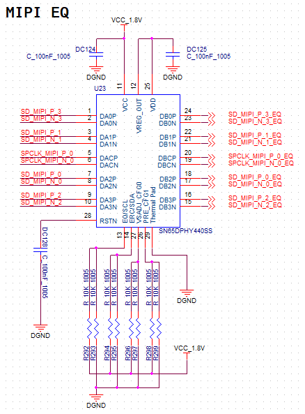
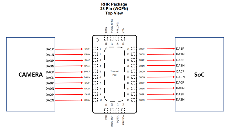
Our customer is routing pcb pattern w/ this part.

They are facing to the issue of crossing MIPI signals.

I think that this device has not a channel swap function.

So I'd like to get confirm whether it is ok or not like below diagram.

I think that is ok.

Could you please give me your feedback?

Best regards,

Michael

  • Michael

    CSI-2 does not have a back channel path. Because of this, there is no requirement on lane ordering as long as the lane order is maintained between the input and the output.

    Please note lane 0 is used for DSI back channel communication. With Lane 0 path (DA0P/N and DB0P/N) supporting bi-directional LP signaling, it is very important that DA0P/N and DB0P/N LP TX is connected to an unterminated LP RX.  If DA0P/ND or B0P/N LP TX is connected to a HS RX, then LP signaling will not be able to reach the LP11 levels and which will cause the DPHY440 to not enable HS data path on Lane0.

    Thanks

    David

  • Hi David,

    Thanks for your kind explain and feedback.

    If CSI-2 interface, you mean that there is no problem on my connection.

    Is it right?

    BR,

    Michael 

  • Michael

    I don't see an issue with the proposed connection itself. But you have to make sure both the camera and SOC DA1P/N have unterminated LP RX since DA1P/N is connected to the DPHY440 lane 0 and lane 0 have LP TX on both DA and DB. If the camera and SOC do not have unterminated LP RX, then you can use DPHY440 I2C register to disable LP and enable HS path only.

    Thanks

    David

  • Hi David,

    Here is actual schematic.

    I will do enable HS mode on all lane and use like schematic.

    Could you finally give me confirm and additional guide?

    BR,

    Michael

  • Michael 

    The design looks fine. To enable HS mode only, please use the following writes to the I2C registers.

    Write Register 0x50 with 8’h1F //Override enable for HS TX path
    Write Register 0x51 with 8’h1F //HS TX path enabled.
    Write Register 0x61 with 8’h00 // Disable LP path.
    Write Register 0x70 with 8’h1F //Override enable for HS RX path
    Write Register 0x71 with 8’h1F // HS RX path enabled.

    Thanks

    David