This thread has been locked.

If you have a related question, please click the "Ask a related question" button in the top right corner. The newly created question will be automatically linked to this question.

DS90UB953-Q1: Dout+/Dout- trace routing for single ended (coax) solution

Part Number: DS90UB953-Q1

Hi,

Requesting your comment on routing of DOUT+ and DOUT- incase of single ended solution

Our schematic snippet: 

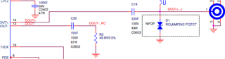
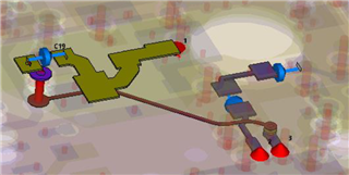
In the layout the traces are routed separately:

DOUT-   between serializer pin 13 and via to GND (bottom layer)

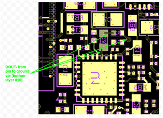
DOUT+ from serializer pin 14, via to layer 8 (with impedance control at 50ohm) and to via to the top layer. 

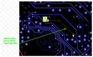
DOUT+ AC cap (c19) to coax connector J1 (top layer)

Please review it.

thanks,

amotz


  • Hi Amotz,

    Here are my comments:

    Which deserializer are you connecting to? In your schematic, C19 = 33nF and C20 = 15nF. This is alright if you are connected to a deserializer that can support Synchronous mode. But if you are connecting to a UB934 or UB913A, then you would need to change these AC coupling capacitor values according to Table 8-3. Design Parameters in the UB953 datasheet.

    The AC coupling capacitors (C19 and C20) should be placed on the same layer and placed as close as possible to the UB953 DOUT+/- pins. This is done in order to minimize the length of the coupled differential trace pair between the pins and the capacitors. C19 should not be placed that far away. 

    In the Layout Examples section of the UB953 datasheet, it states that if DOUT+ is routed on an inner layer, then routing DOUT- loosely-coupled to it will not provide a significant benefit. But if DOUT+ is routed on an outside layer, then there is a significant benefit in routing it alongside the DOUT- trace. Routing the DOUT traces together on an outside layer will introduce a differential nature that will cancel out any common-mode noise that may couple onto the signal traces from the environment. This will improve the EMC performance of your system. The DOUT+/- traces do not need to be length-matched in COAX mode, but you should aim to minimize the trace length that DOUT+ is routed without being loosely-coupled to DOUT-. The traces must also be loosely-coupled (S>3W) in order to prevent each DOUT trace from coupling onto each other.

    Since the DOUT+ trace moves to an inner layer (Layer 8) and then to an outside layer (Top Layer), I recommend that the DOUT- trace be routed alongside DOUT+ all the way up to the connector, in order to improve EMC performance. 

    There are also a number of Layout Guidelines that need to be followed, such as making sure that the DOUT+/- traces are routed over a continuous ground plane in an adjacent layer and to cut-out the ground reference plane underneath the AC coupling capacitor landing pads (C19 and C20) in the adjacent layer. This is not a full Layout Review, since I am unable to provide in-depth analysis with the images you've provided. 

    I recommend also looking at the Layout Guidelines for the connected deserializer (UB960, UB954, etc...) for more visual examples on how to route the DOUT+/- traces on your UB953 board. You can reference how RIN+/- are routed there and implement a similar approach for your UB953.

    Best,

    Justin Phan 

  • Hi Justin,

    Thanks for your answer.

    We are working with 954 at synchronous mode, and already got TI approval for out schematics few month ago.

    I'm adding bellow a 3d illustration of the DOUT+ DOUT- routing to help you perceive the design (for scale understanding, note the c19 is 0402 size).

    Please let me know what material is needed (and how to deliver it confidentially) in order to make it a full Layout Review.

    In this scenario where we need to have the 953 on bottom side and the connector on the top side with with small (~6mm) inner routing and smaller (~4mm) routing on the top side, its not clear how to refer to the recommendation of loosely coupling DOUT+ and DOUT- .Its important for us to know the level of importance of the recommendation of parallel routing of the DOUT- on the (already dense) top layer for a length of only 4mm with the penalty of the added punch of another via to our GND/PWR planes (and keeping in mind we are the receiver only for the low frequency BWD channel).

    thanks,

    amotz


  • Hi Amotz,

    If you are able to provide the layout files (Altium, Cadence, etc...) and schematic to a TI FAE, then they can make a Layout Review request through a TI internal E2E forum post. An Applications Engineer from the FPD-Link team can then be assigned to review the files and return with comments within ~1-2 weeks.

    For now, here are my main comments on the DOUT+/- routing, based on the images that you've provided so far:

    1. Make sure to route DOUT+/- over a continuous ground plane in an adjacent layer.
    2. Both the AC coupling capacitors along DOUT+/- (C19 and C20) must be placed as close as possible to the DOUT+/- pins on the same layer as the UB953.
    3. Verify from the board vendor that the single-ended DOUT+/- traces are 50-Ohms (+/- 10%) impedance.
    4. Remove the ground plane underneath just the AC coupling capacitors' landing pads. This minimizes impedance mismatch.
    5. Since the DOUT+ trace travels along an outside layer, then we strongly recommend that the DOUT- trace be loosely-coupled to the DOUT+ trace, all the way up to the connector. Otherwise, there is a high chance that there will be EMC performance issues that can affect the video data being transferred and negatively affect normal operation. Terminate resistor R2 next to the connector.
    6. There is a PoC circuit and ESD diode in your design. Make sure that the landing pad of the touching Ferrite Bead in the PoC circuit is orthogonal to the DOUT+ trace and not overlapping. Since the DOUT+ trace requires a tightly-controlled 50-Ohm (+/-10%) impedance, we require the landing pad of the Ferrite Bead to just-touch the the DOUT+ trace and to have the reference ground plane underneath the landing pad in an adjacent layer be removed. This minimizes impedance mismatch. We also recommend to do the same for the landing pad of the ESD diode along the DOUT+ trace. See the layout guidelines from the deserializer datasheet for more information. The example below is from the UB960 datasheet. 
      1.   
    7. Make sure the DOUT+ trace can carry the PoC current, without significant temperature increase (<10 degrees Celsius).
    8. The width of the DOUT+/- traces must be the same throughout, in order to prevent impedance mismatch. I noticed that the trace width of the DOUT+ trace increases after the PoC circuit.
    9. The connector landing pattern can introduce impedance mismatch. Recommend to perform a simulation to see if the connector landing pattern maintains 50-Ohms (+/-10%) impedance.
    10. The DAP provides the dominant thermal path for the UB953. Follow the Land Pattern Example in the UB953 datasheet for the even placement of ground vias underneath the device's DAP:

    Best,

    Justin Phan