This thread has been locked.

If you have a related question, please click the "Ask a related question" button in the top right corner. The newly created question will be automatically linked to this question.

DP83867IS: Can't access to register through MDIO

Part Number: DP83867IS
Other Parts Discussed in Thread: USB-2-MDIO

Hi team,

Our customer use this device follow constitutions.

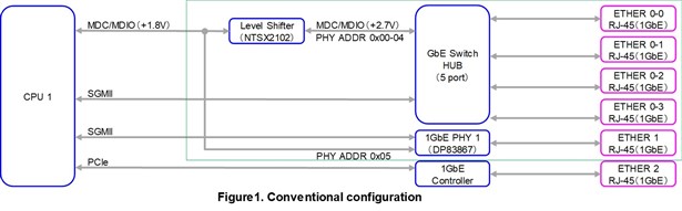
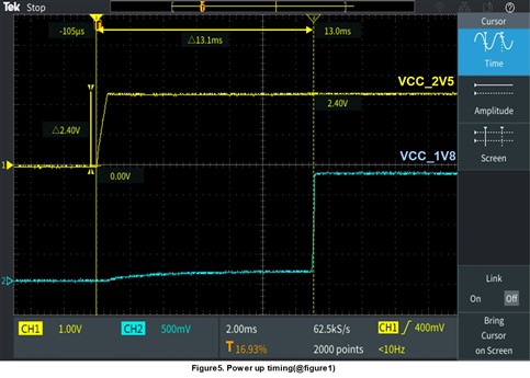
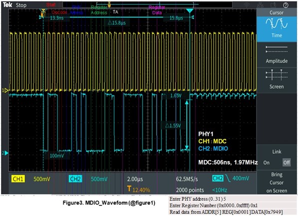
In figure1, we can observe accessing to register of DP83867. Figure3 show the MDIO Register Access at figure1.

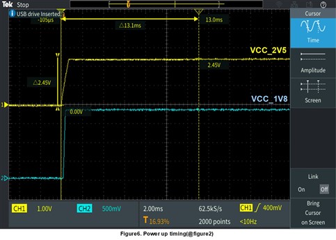
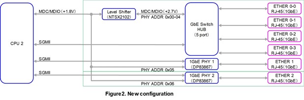
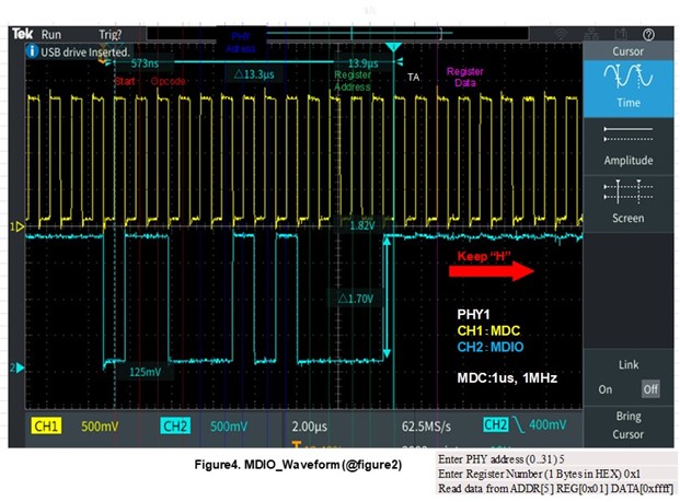
But, in figure2, we can't observe accessing to register of DP83867 at PHY1. Figure4 show the MDIO Register Access at figure2 PHY1.

In figure4, Register Data is 0xffff.


And the customer checked follow.

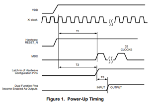
・Config Pin : Strap Configuration waveforms is same when the Reset signal is released in figure1 and figure2

・Clock : The CLK signal to PHY is same in figure1 and figure2.

Please let me know any causes of this matter.

Best regards,

teritama

  • Hi Teritama,

    What is the equivalent PU resistance on MDIO when 2 PHYs are connected? Are there any large stubs on MDIO or MDC lines when the second PHY is added?

    Thanks,

    Lucas

    All information in this correspondence and in any related correspondence is provided “as is” and “with all faults”, and it is subject to TI’s Important Notice (http://www.ti.com/corp/docs/legal/important-notice.shtml).

  • Hi Lucas,

    Thank you for quickly reply.

    >What is the equivalent PU resistance on MDIO when 2 PHYs are connected?
    ⇒We use 4.7kΩ as PU to 1.8V supply on MDIO. The datasheet says "The IEEE specified resistor value is 1.5 kΩ, but a 2.2 kΩ is acceptable.".
     Is 4.7kΩ over acceptable ? 

    >Are there any large stubs on MDIO or MDC lines when the second PHY is added?
    ⇒There are no stubs on MDIO and MDC.

    Best regards,

    teritama 

  • Hi Teritama,

    The recommended PU value is to ensure MDIO is operating at the correct IO voltage level. You can try the recommended 1.5k/2.2k PU and see if this resolves the issue.

    Can you clarify what IO voltage level MDIO is currently at, as well as what is VDDIO between the PHY and CPU? Can you also clarify if you can read PHY2 while PHY1 is active? What if PHY1 is in reset?

    Thanks,
    Lucas

    All information in this correspondence and in any related correspondence is provided “as is” and “with all faults”, and it is subject to TI’s Important Notice (http://www.ti.com/corp/docs/legal/important-notice.shtml).

  • Hi Lucas,

    >The recommended PU value is to ensure MDIO is operating at the correct IO voltage level. You can try the recommended 1.5k/2.2k PU and >see if this resolves the issue.
    ⇒I see. I'll tell the customer to try to use the recommended 1.5k/2.2k PU. However we checked MDIO level is 1.8V in waveform, figure4. 
      Is it possible this resistance is 
    causes of this matter?

    >Can you clarify what IO voltage level MDIO is currently at, as well as what is VDDIO between the PHY and CPU?
    ⇒MDIO level is 1.8V and VDDIO is same 1.8V.

    >Can you also clarify if you can read PHY2 while PHY1 is active? What if PHY1 is in reset?
    ⇒PHY2 can't read when PHY1 is active. And When PHY2 is not connected, PHY1 can't read too.


    we use the supply 1.0/1.8/2.5, Are there some requirement for supply?

    Best regards,

    teritama

  • Hi Teritama,

    Your comment "When PHY2 is not connected, PHY1 can't read too" seems to contradict your original comment "In figure1, we can observe accessing to register of DP83867." Can you clarify whether you can read/write registers when only 1 phy is active?

    This is the requirement for supply ramps in 3-supply mode. Can you also share a supply ramp diagram including reset for your design?

    Thanks,

    Lucas

    All information in this correspondence and in any related correspondence is provided “as is” and “with all faults”, and it is subject to TI’s Important Notice (http://www.ti.com/corp/docs/legal/important-notice.shtml).

  • Hi Lucas,

    We tried the recommend 1.5k/2.2k PU, but didn't resolve. 

    >Your comment "When PHY2 is not connected, PHY1 can't read too" seems to contradict your original comment "In figure1, we can observe >accessing to register of DP83867."Can you clarify whether you can read/write registers when only 1 phy is active?
    ⇒We think too. So we think this issue is strange. In figure2, the schematic of DP83867 is same with figure1. The difference point of DP83867
    configuration between figure1 and figure2 is "two devices are connected to same MDC/MDIO line" and "start up timing of 1.8V supply".
    Follow waveforms show startup timing of 2.5V and 1.8V supply in figure1 and figure2 without RESET.

    If there is some requirement for RESET, let me know.

    Best regards,

    teritama

  • Hi Teritama,

    Can you share the same timing diagram but include reset and MDC lines? You can refer to Figure 1 of the datasheet for reference.

    Thanks,
    Lucas

    All information in this correspondence and in any related correspondence is provided “as is” and “with all faults”, and it is subject to TI’s Important Notice (http://www.ti.com/corp/docs/legal/important-notice.shtml).

  • Hi Lucas,

    We share the timing diagram follow figures. 

    MDC keeps "Low" before start in figure7. In figure8, MDC keeps "Hi" before start.
    Is this possible this difference cause the issue?


     In addition, we could observe the response of PHY in figure2 when use USB to MDIO tool.
    So we think register access timing in CPU to PHY communication maybe concern this issue.

    Is there some requirement with register access timing?

    Best regards,

    teritama 

  • Hi Teritama,

    Based on Fig 1 of the datasheet, MDC should be kept low before startup. Are there any PUs on MDC that could be driving it high?

    Thanks,

    Lucas

    All information in this correspondence and in any related correspondence is provided “as is” and “with all faults”, and it is subject to TI’s Important Notice (http://www.ti.com/corp/docs/legal/important-notice.shtml).

  • Hi Lucas,

    > Are there any PUs on MDC that could be driving it high?
    ⇒Yes, there is 1.0kΩ PU resistance to 1.8V supply. This 1.8V supply is same with MDIO PU. In addition, MDC/MDIO are connected to level translator(NTSX2102) from 1.8V to 2.7V too. The input(1.8V) of this translator is Open-drain, so I think this doesn't influence with this matter.

    Best regards,

    teritama

  • Hi Teritama,

    It looks like MDC is high when it's expected to be low until time T1 (200 ms).

    Can you try removing the PU on MDC so it isn't pulled high before startup?

    Thanks,

    Lucas

    All information in this correspondence and in any related correspondence is provided “as is” and “with all faults”, and it is subject to TI’s Important Notice (http://www.ti.com/corp/docs/legal/important-notice.shtml).

  • Hi Lucas,

    We removed the PU, but the MDC remained high before startup and didn't resolve.

    When use the USB-2-MDIO tool, We can access the register (ADDR5) on PHY1 even though the MDC was high before startup.

    Figure 9 shows the waveform when using the USB-2-MDIO tool.

    Does MDC need to be Low before startup? Do you have other information about MDC/MDIO requirement?


    Best regards,

    teritama

  • Hi Teritama,

    Can you try isolating the PHY from the MAC and using MDC/MDIO with an external launchpad?

    Thanks,

    Lucas

    All information in this correspondence and in any related correspondence is provided “as is” and “with all faults”, and it is subject to TI’s Important Notice (http://www.ti.com/corp/docs/legal/important-notice.shtml).

  • Hi Lucas,

    We checked figure9 waveform using USB-2-MDIO without CPU of figure2. The USB-2-MDIO tool have launchpad "MSP430F5".

    Is this different by "isolating the PHY from the MAC and using MDC/MDIO with an external launchpad" ?

    Best regards,

    teritama

  • Hi Teritama,

    Just to clarify, was the CPU powered off or was there no connection to the PHY? I just want to make sure the MDC line was not affected by the CPU at all.

    Thanks,

    Lucas

    All information in this correspondence and in any related correspondence is provided “as is” and “with all faults”, and it is subject to TI’s Important Notice (http://www.ti.com/corp/docs/legal/important-notice.shtml).

  • Hi Lucas,

    The condition is follow.

    ・CPU is connected to PHY.
    ・MDC/MDIO at CPU side is Open-Drain.
    ・The MDIO access from CPU side is stop. Maybe the power was on.

    In this condition, we achieved the access to ADDR5 when use USB-2-MDIO tool. 

    Best regards,

    teritama

  • Hi Teritama,

    Apologies for the repeated questions, I want to clarify again.

    Regardless of whether using the CPU or external launchpad to read registers, you are able to access the PHY 1 (addr 5) but not PHY 2 (addr 2). 

    Have we confirmed PHY 2 is active and in a "normal operation" state? Do you see a clockout signal or RX_CLK signal? Do you see MDI link pulses after power on? If we swap PHY 2 with PHY 1 in Figure 1 (the single PHY configuration from the original post) are we able to read the registers of PHY 2?

    Thank you,

    Nikhil Menon

    Applications Engineer | Ethernet

    All information in this correspondence and in any related correspondence is provided “as is” and “with all faults”, and it is subject to TI’s Important Notice (http://www.ti.com/corp/docs/legal/important-notice.shtml).

  • Hi Nikhil,

    Thank you for reply.

    >Regardless of whether using the CPU or external launchpad to read registers, you are able to access the PHY 1 (addr 5) but not PHY 2 (addr 2). 
    ⇒we could achieve the access even the PHY2(addr6) when used USB-2-MDIO tool. And in fugure1, we able to read the register of PHY2 as well.

    >Do you see a clockout signal or RX_CLK signal?
    ⇒We don't use CLK_OUT and Rx_CLK. Do these CLK have to be used in double PHY configuration(Figure2)?

    >Do you see MDI link pulses after power on?
    ⇒We don't see MDI pulses waveform.

    Best regards,

    teritama

  • Hi Teritama,

    Apologies, RX_CLK will be unused for SGMII mode. I asked to view CLK_OUT to make sure PHY is in a normal operational state. If in a normal operating condition, the CLK_OUT signal will be present and register access should be available. This will be an indication that you should be able to read/write registers. 

    Is there any difference in MDC waveform when using USB-2-MDIO tool via external launchpad vs when using CPU? Please make sure CPU is disconnected when probing the MDC waveform for USB-2-MDIO.

    MDI link pulses should be present if device is in a normal operational mode without link. Are both PHYs powered at the same time? Is there any change if one PHY is powered some time (let's say 1-2 seconds) after the other?

    Thank you,

    Nikhil

    All information in this correspondence and in any related correspondence is provided “as is” and “with all faults”, and it is subject to TI’s Important Notice (http://www.ti.com/corp/docs/legal/important-notice.shtml).

  • Hi Nikhil,

    > If in a normal operating condition, the CLK_OUT signal will be present and register access should be available.
    ⇒I see. I'll check to the customer if be able to view CLK_OUT signal. 

    >Is there any difference in MDC waveform when using USB-2-MDIO tool via external launchpad vs when using CPU?
    >Please make sure CPU is disconnected when probing the MDC waveform for USB-2-MDIO.
    ⇒There are no difference in MDC waveform both of condition when using USB-2-MDIO tool vs when using CPU.
     And we can't isolate CPU, because the pattern of CPU2 to PHY is connected in the inside layer. When use USB-2-MDIO tool, we stopped the MDIO of CPU2 by this terminal being Open-drain. 

    >Are both PHYs powered at the same time?
    ⇒Yes, PHY1 and PHY2 are powered at same time. And power up timing for each voltage(2.5V, 1.0V, 1.8V) is same between CPU2 and USB-2-MDIO tools. 

    >Is there any change if one PHY is powered some time (let's say 1-2 seconds) after the other?
    ⇒I'll check to the customer. Should we delay the time at all power supply(2.5V, 1.0V, 1.8V)?

    Best regards,

    teritama

  • Hi Teritama,

    Responding to your points below:

    There are no difference in MDC waveform both of condition when using USB-2-MDIO tool vs when using CPU.
     And we can't isolate CPU, because the pattern of CPU2 to PHY is connected in the inside layer. When use USB-2-MDIO tool, we stopped the MDIO of CPU2 by this terminal being Open-drain. 

    Does this mean we still see that MDC is pulled high until it starts oscillating? I understand about PHY connection to CPU being on inside layer. Keeping both MDC/MDIO as Open-drain should be ok.

    Is there any change if one PHY is powered some time (let's say 1-2 seconds) after the other?
    ⇒I'll check to the customer. Should we delay the time at all power supply(2.5V, 1.0V, 1.8V)?

    Please delay all supplies to PHY 2 until PHY 1 has fully ramped and powered on (wait 1-2 seconds).

    Thank you,

    Nikhil

    All information in this correspondence and in any related correspondence is provided “as is” and “with all faults”, and it is subject to TI’s Important Notice (http://www.ti.com/corp/docs/legal/important-notice.shtml).

  • Hi Nikhil,

    >Does this mean we still see that MDC is pulled high until it starts oscillating? 
    ⇒Yes, before MDC starts, MDC is pulled high. But, when using USB-2-MDIO tools, we can  access the register(ADDR5) on PHY1 even though the MDC was high before startup.

    >Please delay all supplies to PHY 2 until PHY 1 has fully ramped and powered on (wait 1-2 seconds).
    ⇒I see. I'll let you know as soon as check the result.

    We checked the CLK_OUT and MDI link at the three cases,figure1 configuration, figure2 configuration(CPU) and figure2 configuration(USB-2-MDIO).
    In any case, we can see the CLK_OUT output 25MHz clock and PHYs can be 1000BASE-T/Full Link.

    Best regards,

    teritama

  • Hi Teritama,

    Thanks for confirming MDC waveform is the same whether using USB-2-MDIO or the CPU

    Considering CLKOUT is present and PHYs are linking up I think there is no need to check the MDI link pulses, as we have already confirmed that the PHY is operating as expected on the MDI side. 

    Please do let me know the results of powering up one PHY after the other. 

    Thank you,

    Nikhil

    All information in this correspondence and in any related correspondence is provided “as is” and “with all faults”, and it is subject to TI’s Important Notice (http://www.ti.com/corp/docs/legal/important-notice.shtml).

  • Hi Nikhil,

    The power up timing on PHY1 and PHY2 couldn't change, because these power line is same each other.
    we checked the access in below condition, but PHY1 couldn't access.

    ・PHY1 is connected to CPU2
    ・PHY2 is disable with MDIO/MDC is not used
    ・The power of PHY1 and PHY2 is supplied on same timing.

    Addition, the customer became to be able to access CPU2 to PHY1 and PHY2 by below way. 

    They use a 10ohm damping resister on MDC line. When they change this dumping resistor to 62ohm, they was able to access CPU to PHYs.

    Below figure shows the MDC fall down waveform of PHY1 that using 10ohm dumping resister and 62ohm dumping resister.

    I think this wave form difference is caused by impedance is match or don't match.

    Do you think it is possible this difference cause this matter?

    note: On PHY2, the waveform is same. Using 4.7k ohm PU on MDIO/MDC line.

    Best regards,

    teritama 

  • Hi Teritama,

    We are reviewing this information internally and will have additional feedback by Monday of this week.

    Thank you,

    Nikhil

    All information in this correspondence and in any related correspondence is provided “as is” and “with all faults”, and it is subject to TI’s Important Notice (http://www.ti.com/corp/docs/legal/important-notice.shtml).

  • Hi Nikhil,

    I see. Please let me know if you have some update.

    In addition, the customer checked the waveform when the level translator(NTSX2102) connected to MDC/MDIO is disable.
    We could observe the access to MDIO when both damping resister 10Ω and 62Ω.

    I think this level shifter's condition is related to this matter.

    Please some comment about this too.

    Best regards,

    teritama

  • Hi Teritama, 

    It looks like when a 10 ohm damping resistor was used, there was some glitch in the MDC waveform, where the waveform quickly increases again before ramping down to 0. This could be the cause of some error accessing MDC/MDIO. In your most recent post you mention "We could observe the access to MDIO when both damping resistor 10Ω and 62Ω." Does this mean you now have register access for both damping resistors?

    It's possible the level shifter is placing some additional loading on the MDC/MDIO lines. Can you provide a schematic of the level shifter circuit?

    Thank you,

    Nikhil

    All information in this correspondence and in any related correspondence is provided “as is” and “with all faults”, and it is subject to TI’s Important Notice (http://www.ti.com/corp/docs/legal/important-notice.shtml).

  • Hi Nikhil,

    >Does this mean you now have register access for both damping resistors?
    ⇒Yes, when the level shifter is disable, we have register access for both damping register. When  the level shifter is enable, we couldn't have access for only 10 ohm damping register.

    >Can you provide a schematic of the level shifter circuit?
    ⇒Follow figure is the schematic. EMI1_MDC_18 and EMI_MDIO_18 ports are connected to CPU and PHY.

    Best regards,

    teritama 

  • Hi Teritama,

    Any particular reason why a different value chosen for MDC vs MDIO pull ups on both the A and B side of the level shifter? If I'm understanding correctly, the damping resistor would be in series with the MDC/MDIO lines, correct?

    Thank you,

    Nikhil

    All information in this correspondence and in any related correspondence is provided “as is” and “with all faults”, and it is subject to TI’s Important Notice (http://www.ti.com/corp/docs/legal/important-notice.shtml).

  • Hi Nikhil,

    >Any particular reason why a different value chosen for MDC vs MDIO pull ups on both the A and B side of the level shifter?
    ⇒I'll check to the customer if there  is any reason this pull up setting. Is it possible this pull up mismatch cause any issue?

    > If I'm understanding correctly, the damping resistor would be in series with the MDC/MDIO lines, correct?
    ⇒Yes, you saying correct. the damping resister is in series with the MDC/MDIO line.

    Best regards,

    teritama

  • Hi Teritama,

    The strength of the pull resistor will determine how closely tied the signal is to the supply rail. There is a small possibility that having pull ups of different strengths (it looks like there is a 3x difference here) leads to enough of a difference in the signal levels between MDC and MDIO to cause issues, hence why a damping resistor in series may help. Though these should be a fairly robust interface. Please let me know if using the same pull-up values for both MDC and MDIO help resolve this issue.

    Thank you,

    Nikhil

    All information in this correspondence and in any related correspondence is provided “as is” and “with all faults”, and it is subject to TI’s Important Notice (http://www.ti.com/corp/docs/legal/important-notice.shtml).

  • Hi Nikhil,

    Thank you for comment.

    I asked to the customer to check if this issue is resolved by pull up resistor replace.

    Please wait the result.

    Best regards,

    teritama

  • Hi Teritama,

    Thanks for the update. Please keep me posted!

    Thank you,

    Nikhil

    All information in this correspondence and in any related correspondence is provided “as is” and “with all faults”, and it is subject to TI’s Important Notice (http://www.ti.com/corp/docs/legal/important-notice.shtml).

  • Hi Nikhil,

    We checked result when the pull up resister MDC/MDIO are replaced to same 4.7kohm at both of case the damping resister is 10ohm and 62ohm.

    The issue didn't resolve. We observed the waveform same figure9 and figure10 of this thread.

    Best regards,

    teritama

  • Hi Teritama,

    Given that the issue is resolved when the level shifter is disabled, it looks to be an issue involving the level shifter and this becomes difficult to debug from a PHY perspective. Is the series damping resistor an acceptable working solution?

    Thank you,

    Nikhil

    All information in this correspondence and in any related correspondence is provided “as is” and “with all faults”, and it is subject to TI’s Important Notice (http://www.ti.com/corp/docs/legal/important-notice.shtml).

  • Hi Teritama,

    I am covering for nikhil. Do you have some inputs or questions. If not can i close the thread ?

    Regards,

    Sreenivasa

  • Hi Teritama,

    I am covering for nikhil. Do you have some inputs or questions. If not can i close the thread ?

    Regards,

    Sreenivasa

  • Hi Sreenivasa, nikhil,

    Apologies, late the reply.

    Thank you for your kind support for a long term, it's no problem close the thread.

    Best regards,

    teritama

  • Hi Teritama,

    Noted and thank you.

    Regards,

    Sreenivasa