This thread has been locked.

If you have a related question, please click the "Ask a related question" button in the top right corner. The newly created question will be automatically linked to this question.

TDP158: Have no BIOS screen shown when TDP158 connected from M/B to Monitor

Part Number: TDP158

Hi Sirs,

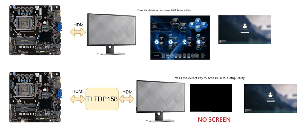
My customer used the TDP158 to develop an HDMI re-driver board(HDMI RX side has pull-up 49.9Ohm to 3v3), when they connected TDP158 from M/B(Intel H410 chipset) to Monitor, there is no BIOS screen shown.

If they connected M/B to Monitor directly, the BIOS will be displayed, you can refer to the setup description as below figure.

How to fix this issue? please advise. Thanks!

  • Hi,

    Can you please send the schematic for review? Can you please measure the TDP158 clock output? 

    For this particular application, the DP159 will be a better choice than the TDP158 with its adaptive equalizer. Any chance they can replace DP158 with DP159? Please see this app note on the implementation difference between the two, https://www.ti.com/lit/ug/sllu291a/sllu291a.pdf.

    Thanks

    David 

  • Hi Sir,

    Can you please send the schematic for review? => see the below attachment, you could see the customer has not add 49.9ohm pull high to 3.3V for HDMI input in the schematics. but they have try to add them on our board , but still not work for our issue.

    Satunr_KVM interface board_20201221.pdf

    Can you please measure the TDP158 clock output? => The customer can not measured any clock output when the BIOS no screen output.

  • Hi,

    1. Is the TDP158 being designed on the motherboard or the monitor? The schematic shows CN3 and CN4 connector and they do not follow the standard HDMI connector pinout. Are they using a custom cable to connect between the motherboard and the monitor? If they do, are they mapping the HDMI pinout correctly in the custom cable?

    2. What is the VCC voltage? If VCC is 5V, you can't pull SDA_SRC and SCL_SRC to 5V as this will exceed the absolute maximum rating (-0.3 to 4V) on these two pins.

    3. Motherboard should already have 2k pullup and sink should have 47k pullup. So I would recommend

    a. Removing pullup resistors on SDA_SRC, SCL_SRC, SDA_SNK, and SCL_SNK

    b. Pull SDA_SRC and SCL_SRC to ground

    c. Tie SDA_SNK and SCL_SNK signal directly between the CN3 and CN4

    d. Tie TDP158 SDA_SNK and SCL_SNK directly to the SDA_SNK and SCL_SNK bus between CN3 and CN4

    4. TERM pin needs to be left floating

    5. EQ0 and EQ1 need to be tuned to compensate for the loss

    We definitely need to measure the clock output in order to further debug this issue.

    Thanks

    David