This thread has been locked.

If you have a related question, please click the "Ask a related question" button in the top right corner. The newly created question will be automatically linked to this question.

DP83867IS: DP83867 PHY Configure Wake on LAN

Expert 1600 points
Part Number: DP83867IS
  • My board contains 2 DP83867IS connected back-to-back (PHY ADDR = 00000 and 00001 respectively).
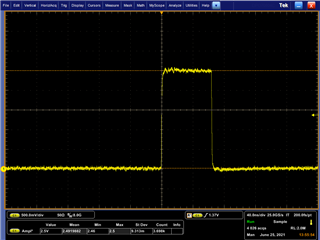
  • The First is supposed to implement the Wake-On-LAN feature (output to INT/PWDN pin).

My question is:

  • what are the necessary registers I'm supposed to write (since Pwr-on-reset) to get this function to work properly?
  • Does the order of writing these registers matter? 

Here is what I configured so far through the MDIO  interface.

#OPCODE (2)

PHY_ADDR (5)

REG_ADDR(5)

REG_DATA(16)

Total Word (28) bits

Instruction

Comment

[MANDATORY] - BMCR, RXFCFG, and MICR Registers are essential for device configuration and WoL setup

01

00000

00000

0001000101000000

0x04001140

Write U39's BMCR to 0x1140

Section 8.3.1
Please ensure that BMCR (register address 0x0000) bit[10] is disabled, when using the
WoL feature. This bit enables the MII ISOLATE function used to disable the MAC interface
of the PHY, also disabling the WoL interrupt on this PHY.

BIT 6, 13 SPEED SELECTION LSB 0, RW Speed Select (Bits 6, 13):
When auto-negotiation is disabled writing to this bit allows the port speed to be selected.
11 = Reserved, 10 = 1000 Mbps, 1 = 100 Mbps, 0 = 10 Mbps
BIT12 AUTO-NEGOTIATION ENABLE Strap, RW Auto-Negotiation Enable:
Strap controls initial value at reset.
1 = Auto-Negotiation Enabled - bits 8 and 13 of this register are ignored when this bit is set.
0 = Auto-Negotiation Disabled - bits 8 and 13 determine the port speed and duplex mode.

01

00001

00000

0001000101000000

0x04201140

Write U40's BMCR to 0x1140

01

00000

01101

0000000000011111

0x040D001F

Write register 0x0134 to value 0x00A1 .
1. Write register 0x0D to value 0x001F.
2. Write register 0x0E to value 0x0134
3. Write register 0x0D to value 0x401F.
4. Write register 0x0E to value 0x00A1.

Section 8.3.1.3
Wake-on-LAN functionality is configured through the RXFCFG register (address 0x0134).

BIT 10:9 WOL_OUT_STRETCH 00, RW Wake-on-LAN Output Stretch:
If WoL out is configured for pulse mode, the pulse length is defined as the following number of 125-MHz clock cycles: 11 = 64 clock cycles, 10 = 32 clock cycles, 01 = 16 clock cycles, 00 = 8 clock cycles

BIT 8 WOL_OUT_MODE 0, RW Wake-on-LAN Output Mode:
1 = Level Mode. WoL is cleared by a write to WOL_OUT_CLEAR (bit 11).
0 = Pulse Mode. Pulse width is configured via WOL_OUT_STRETCH (bits 10:9).


BIT7 ENHANCED_MAC_SUPPORT 0, RW Enable Enhanced Receive Features:
1 = Enable for Wake-on-LAN, CRC check, and Receive 1588 indication.
0 = Normal operation.


SCRON_EN 0, RW Enable SecureOn Password:
1 = SecureOn Password enabled.
0 = SecureOn Password disabled.

01

00000

01110

0000000100110100

0x040E0134

01

00000

01101

0100000000011111

0x040D401F

01

00000

01110

0000000010100001

0x040E00A1

01

00000

10010

0000000000001000

0x04120008

Write U39's MICR to 0x0008

3 WOL_INT_EN: Enable Wake-on-LAN Interrupt:
1 = Enable Wake-on-LAN Interrupt.
0 = Disable Wake-on-LAN Interrupt.

# [HIGHLY RECOMMENDED] - Set a password to be embedded in the Magic Pattern to wake up the PHY (Register: RXFSOP1,2,3)

01

00000

01101

0000000000011111

0x040D001F

Write register 0x0139 to value 0x0000 .
1. Write register 0x0D to value 0x001F.
2. Write register 0x0E to value 0x0139
3. Write register 0x0D to value 0x401F.
4. Write register 0x0E to value 0x0000.

8.6.55 SecureOn Pass Register 2 (RXFSOP1,2,3)

Password can be any 3 x 16 bit word

01

00000

01110

0000000100111001

0x040E0139

01

00000

01101

0100000000011111

0x040D401F

01

00000

01110

0000000000000000

0x040E0000

01

00000

01101

0000000000011111

0x040D001F

Write register 0x013A to value 0x0000 .
1. Write register 0x0D to value 0x001F.
2. Write register 0x0E to value 0x013A
3. Write register 0x0D to value 0x401F.
4. Write register 0x0E to value 0x0000.

01

00000

01110

0000000100111010

0x040E013A

01

00000

01101

0100000000011111

0x040D401F

01

00000

01110

0000000000000000

0x040E0000

01

00000

01101

0000000000011111

0x040D001F

Write register 0x013B to value 0x0000 .
1. Write register 0x0D to value 0x001F.
2. Write register 0x0E to value 0x013B
3. Write register 0x0D to value 0x401F.
4. Write register 0x0E to value 0x0000.

01

00000

01110

0000000100111011

0x040E013B

01

00000

01101

0100000000011111

0x040D401F

01

00000

01110

0000000000000000

0x040E0000

  • Hello,

    It will take me a couple of days to go through all of your settings and confirm. I will get back to you by the end of business Wednesday (9/1).

    Kind Regards,

    Joe

    All information in this correspondence and in any related correspondence is provided “as is” and “with all faults”, and is subject to TI’s Important Notice (www.ti.com/.../important-notice.shtml)

  • Hello,

    Here is an example script used for WoL where I output the WoL pulse to GPIO_0 using a DP83867ERGZ-R-EVM Evaluation board | TI.com.

    I have verified the WoL functionality with the pattern starting at byte 62. I have included the script I used when writing to the DP83867. For further verification, I captured the WoL pulse on the GPIO_0 Pin after configuring register 0x0172. I also configured register 0x0134 to 0x0082, configuring the WOL_OUT_MODE for pulse. These are the necessary registers for the WoL feature of the DP83867 without a password in the magic packet.


    // Title: DP83867 WoL Test
    // Company: Texas Instruments
    // Location: Santa Clara, CA
    // Developer: Joe Vanacore
    // Date: June 8, 2021
    // Customer Debug for WoL
    // Texas Instruments
    
    begin
    
    //delay 100
    //0000 2100	// force 100Mbps, full-duplex
    013C 475f	//Pattern Bytes 0 and 1
    013d 0e0c	//Pattern Bytes 2 and 3
    013e 4bfb	//Pattern Bytes 4 and 5
    013f 641d	//Pattern Bytes 6 and 7
    0140 0000	//
    0141 0000	//
    0142 0000	//
    0143 0000	//
    0144 0000	//
    0145 0000	//
    0146 0000	//
    0147 0000	//
    0148 0000	//
    0149 0000	//
    014a 0000	//
    014b 0000	//
    014c 0000	//
    014d 0000	//
    014e 0000	//
    014f 0000	//
    0150 0000	//
    0151 0000	//
    0152 0000	//
    0153 0000	//
    0154 0000	//
    0155 0000	//
    0156 0000	//
    0157 0000	//
    0158 0000	//
    0159 0000	//
    015a e649	//Pattern Bytes 60 and 61
    015b fb54	//Pattern Bytes 60 and 61
    015c 0000	//Byte Mask 0 to 15
    015d 0000	//Byte Mask 16 to 31
    015e 0000	//Byte Mask 32 to 47
    015f 0000	//Byte Mask 48 to 63
    0161 0000	//Pattern start point (62 decimal)
    0172 0033	//Configures GPIO_0 pin for WoL Indication
    0134 0082	//WoL on pattern enabled, level Indication, pulse mode
    
    end

    I then configured SmartBits with the following pattern for generation to verify WoL functionality:

    Please let me know if you need any further clarification.

    Kind Regards,

    Joe

    All information in this correspondence and in any related correspondence is provided “as is” and “with all faults”, and is subject to TI’s Important Notice (www.ti.com/.../important-notice.shtml)

  • Hi Joe, 
    Thank you so much for this detailed answer. I just want a bit of confirmation/clarification for these points, because we have very limited flash space for this initialization routine in our application and we want to make this initialization sequence as short as possible:

    • All of these registers that should be set to 0000, I understood from the datasheet their default values are already zero, so can I skip these commands?
    • We don't need to configure pattern registers bits 0 to 63 if we are using the WoL on Magic Pattern setting. Instead, we may "optionally" configure RXFSOP1,2,3 (while setting Bit 5 of 0x0134).
    • If using the INT pin instead of GPIO, we should write 0x0012 (MICR) to 0x0008 instead of writing  0x0172 to value 0x0033.

    Thank you again

  • Hello,

    Can you kindly confirm which registers you are referring to be set to 0x0000?

    Kind Regards,

    Joe

    All information in this correspondence and in any related correspondence is provided “as is” and “with all faults”, and is subject to TI’s Important Notice (www.ti.com/.../important-notice.shtml)

  • 0140 0000	//
    0141 0000	//
    0142 0000	//
    0143 0000	//
    0144 0000	//
    0145 0000	//
    0146 0000	//
    0147 0000	//
    0148 0000	//
    0149 0000	//
    014a 0000	//
    014b 0000	//
    014c 0000	//
    014d 0000	//
    014e 0000	//
    014f 0000	//
    0150 0000	//
    0151 0000	//
    0152 0000	//
    0153 0000	//
    0154 0000	//
    0155 0000	//
    0156 0000	//
    0157 0000	//
    0158 0000	//
    0159 0000	//
    
    015c 0000	//Byte Mask 0 to 15
    015d 0000	//Byte Mask 16 to 31
    015e 0000	//Byte Mask 32 to 47
    015f 0000	//Byte Mask 48 to 63
    0161 0000	//Pattern start point (62 decimal)

    These ones for example (or any register that has its default value=0 in the Datasheet).

  • Hello,

    Any register with default value of 0x0000, you do not need to write to.

    As far as the pattern byte registers, if your pattern has these bytes as 0 then you do not need to write to these registers.

    If in the future you want nonzero values, then you will have to write to these registers. 

    Kind Regards,

    Joe

    All information in this correspondence and in any related correspondence is provided “as is” and “with all faults”, and is subject to TI’s Important Notice (www.ti.com/.../important-notice.shtml)