


Other Parts Discussed in Thread: TPS55288, TPS65988
Dear sir,
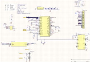
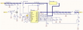
I have encountered the problem about the TPS65987D’s internal power MOSFET broken during loading out around 4.8A, 20V. My design is mainly referenced to the TPS65987EVM and TPS55288 is used as buck boost converter which connects to the TPS65987D by I2C. In addition, only PP_HV2 power path is enabled for DFP configuration. Please see the schematics below. 5V, 9V, 15V and 20V PDOs are broadcasted once the USB loading plugs in. The input voltage to the TPS55288 is 25.2V.
During debug process, E-mark cable was used and the PDO 20V 5A was selected. At the beginning, the USB loading started to load 3A first and the loading current slowly increase. Until reached to 4.8A, output voltage drops and the loading current became zero.
I found that the internal MOSFET of TPS65987D has broken out. Besides, the CC1 and CC2 couldn’t communicate to the loading any more. However, its I2C communication to the TPS55288 still works with. The TPS65987D’s LDO_3V3, LDO_1V8 also alive.
Why did the internal MOSFET burn out at 4.8A? Should the hardware design need to change to duo power mode configuration for 5A? The TPS55288 part seems to work fine after this issue.
Why CC1 and CC2 couldn’t communicate after that? Actually, except for the communication, CC pins could still pull down to 1.6V when it connected to the USB loading after this issue.
Is the problem related to the E-mark cable? However, 5V supply has already supplied to the pp_cable pin for VCONN in my design. Or the layout problem?
Please help to give me some hints.
Thank you!
Best regards!
Alan
