This thread has been locked.

If you have a related question, please click the "Ask a related question" button in the top right corner. The newly created question will be automatically linked to this question.

DP83TD510E-EVM: MSP430 - USB example - driver issue - Win7 x64

Part Number: DP83TD510E-EVM
Other Parts Discussed in Thread: USB-2-MDIO, DP83TD510E, DP83822I

Hello,

Here is my configuration : The DP83TD510E-EV  board is connected with USB plug. I strap R24 as recommended and the jumper USB 5v is on.

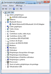
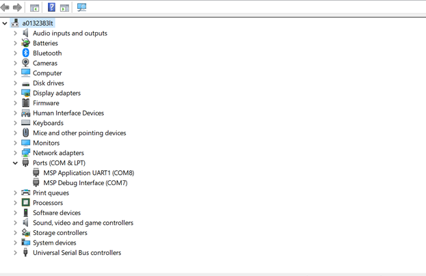
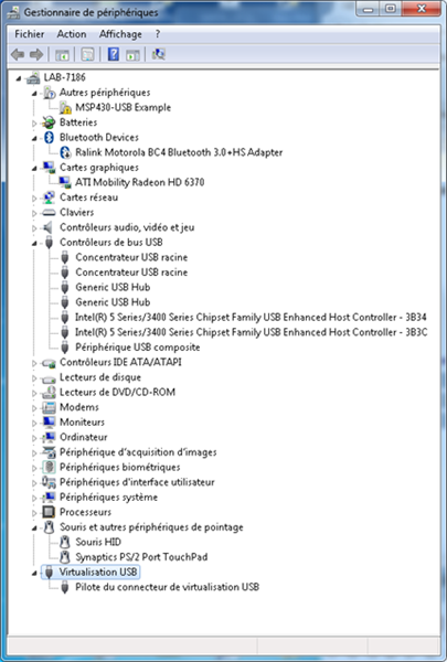
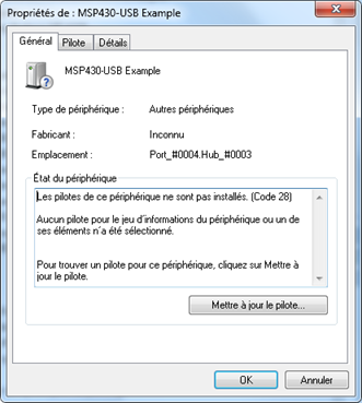
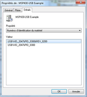
The board power led's are on. USB is plugged on the PC and the device management panel on Win7 see the MPS430 usb example board with (!). 

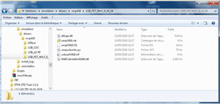
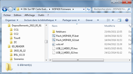
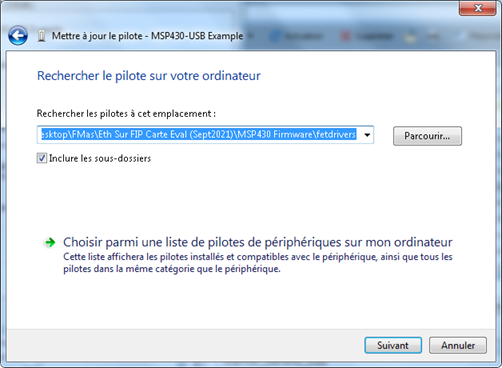
as I up date the driver and point out through the driver I did download the package fetdrivers from the link from the guide and from here : MSP430_FET_Drivers 1_0_1_1 - TI.com

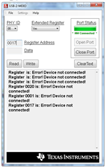
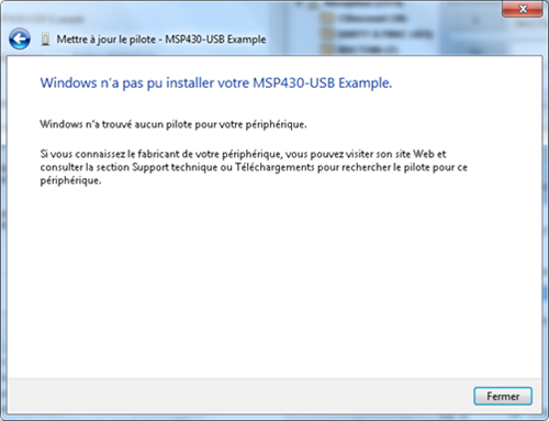
After installing the package Win7 refused to install the driver as I try to update the MSP430 driver, Win7 says : "No driver has been found on your computer."....

Could you confirmed me about the driver link I use to download the setup driver ?

is this issue known already ?

Thx

Fab

  • Hello Fab, 

    Thank you for the query.

    We are not aware of any issues related to installing the drivers.

    Would it be possible for you to check on a different version of windows.

    In the mean time, i will also check if we have some inputs.

    Regards,

    Sreenivasa

  • Hello Fab, 

    Good morning.

    Did you trying using the USB to MDIO without updating the firmware using the USB 2 MDIO?

    Do you see the USB device recognized?

    Regards,

    Sreenivasa

  • Hello Sreenivasa

    I only have Win7 PC x64 for this board 511e connection. 

    About the installed driver:

    I download the driver (snlu271A.pdf - guide link :  software-dl.ti.com/.../index_FDS.html.) I have driver in : msp430/USB_FET_Win7_8_10_64/ in that folder I have file:  usbuart3410.inf . In this file in section [TI.Section.NTia64] the device name is USB\VID_0451&PID_xxxx
    After plugging the board on the USB PC the name in the "peripheries management"   is " MSP430-USB Example". When I open the properties on this MPS430 the hardware ID device is :

    USB\VID_2047&PID_0300.

    When Win7 tries to install the driver it found no driver available that match the hardware, isn't it normal ?

    the goal is to establish the communication (same way I did with 2 boards 811E ), I probably need to turn 1 board 511E in master and 1 board 511E in slave mode linked with 1 twisted pair. Do I need to do this configuration (M/S) with the SW USB-2-MDIO Tool ? An so the need to correctly install the USB 511 driver ?

    Thx

    Best regards

    Fabrice

  • another thing : The guide tells that resistors and strap need to be modify (hardware modification) and in the same time ther is a software programming :

    *DP83TD510E
    – Write register 0x0017[5]=1
    – Write register 0x0017[7]=0
    * DP83822I
    – Write register 0x0017[5]=1
    – Write register 0x0017[7]=1

    Do you need to do both HW modifications AND SW programming or is it HW OR SW modifications to turn in M/Slave  mode boards ?

    Fabrice

  • Hello Fab, 

    Before you try the above, can you please check the below. 

    (13) DP83TD510E-EVM: MSP430_FET_Drivers are not installing - Interface forum - Interface - TI E2E support forums

    Not sure why the link does not worr, sorry about that. Please see below.

    replace R24 with a 0 Ohms Resistor to power it only through the USB-Port, 

     Please check the DC voltage across C62 and C70.

    Check the clock at R149

    Perform a reset using S4.

    Further debug:

    If there is no clock on R149 it Seems like the DP83822 is getting no clock signal at all.  You may need to check configuring the register through MDIO interface.

    USB-2-MDIO 

    3.4 SMI Connection

    In Media Converter configurations, the MDIO/MDC lines of the DP83TD510E and DP83822I are tied together. Both PHYs can be accessed simultaneously. The DP83TD510E has been set to PHY address 00 and the DP83822I has been set to PHY address 05.  Connect micro-USB to J4

    Please go through the section 4 Software of the user guide.

    In default state the DP83TD510E register 0x0017 bit 7 is set to "XI is 50Mhz". Change that to "XI is 25Mhz" and it will result in a clock signal on R149. 

    In short: Write "4021" to the register "0017" on the DP83TD510E and you will be able to communicate to the DP83822 over SMI.

    (+) DP83TD510E-EVM: can't establish link - Interface - INTERNAL forum - Interface - INTERNAL - TI E2E support forums

    Regards,

    Sreenivasa

  • Hello,

     The first link is related to an issue with powering from USB only, to solve it you have to power both USB plugg and external DC from J12 => I have already solved it. Also, I do not have pkg drivers installation issue but Win7 recognition driver issue. files were copying ok on the PC but these files semses to me the wrong one for MSP430 - USB board.

    On going :

    Replace R24 with a 0 Ohms Resistor to power it only through the USB-Port,  => I've done it last week, the HW devise is  ok an well visible on Win7 with the name "MSP430..." (see below)  in "the devices management" win7 panel with (!) sign because of the driver not installed properly (or bad one).

     Please check the DC voltage across C62 and C70.  => please send me the schematic and components name placement (native pdf) on the board so I can proceed with automatic research (not image), the guide provide just a low quality image  and I can't do any research on it, it is so impossible or very difficult to find any component names. What should be the DC voltage on C62 and C70 ?

    Check the clock at R149 => What do I found ? Hz / level

    About register with MDIO  : If I need to connect the board to my PC with USB plug do I need to install driver first ?

    The USB-2-MDIO SW is well installed but any PHY ID I select it shows the message :

    Error Device not connected

    In the setting I choose the USB port (3 as default ? ) and speed 9600bps.

    the PHY ID I  select is 0 (guide §3.7) and I try to read register 0017  :

    I think I do not have the correct driver to access to the board with the USB-2-MDIO SW :  The MSP430 - USB device still unrecognized because of the wrong driver. 

    here is what I did install last week :  why the pic quality is so poor ?

    best regards

    fabrice

  • Hello Jo, 

    Please check available  ports as below 

    I set the port as com8. 

    DP83TD510E has been set to PHY address 00

    Extended registers - set it to No.

    Please try reading the registers.

    Regards,

    Sreenivasa

  • I do not have "MSP appli UART or debug" on Port COM , in fact no port com is loaded on my PC. When I remove the HW 511 board, the MSP430 (!) disappear from the management devices panel :

    The issue is : wrong driver for this 511 board. Please send me the correct driver for win7 x64.

  • Hi Sreenivasa

    Could you just reply on these simple questions please :

    1) Do I need to configure one board 511 in master mode and one board in slave mode to communicate through a twisted pair as it is with 811e board ?

    Your Answer (Sreenivasa) :  Y/N

    2) If Yes : To configure Master or Slave Do I need to modify ONLY  hardware components from the board, as explain from the guide §3.2 ?

    Your Answer (Sreenivasa) :  Y/N

    3) If NO : To configure Master or Slave mode : Do I need to proceed ALSO (+HW ) with the software configuration from the guide ?

    Your Answer (Sreenivasa) :  Y/N

    4) If NO : To configure Master or Slave mode : Is the SW configuration enough instead of HW modifications ? 

    Your Answer (Sreenivasa) :  Y/N

    Thx

    Bets regards

  • Hello Fab, 

    The section 3.2 is for configuring the RMII master or slave mode. 

    DP83TD510E in RMII Master Mode, DP83822I in RMII Slave Mode (default)

    All you have to do is the below if there is no 50MHz clock on R149.

    3.4 SMI Connection

    In Media Converter configurations, the MDIO/MDC lines of the DP83TD510E and DP83822I are tied together. Both PHYs can be accessed simultaneously. The DP83TD510E has been set to PHY address 00 and the DP83822I has been set to PHY address 05.  Connect micro-USB to J4

    Please go through the section 4 Software of the user guide.

    In default state the DP83TD510E register 0x0017 bit 7 is set to "XI is 50Mhz". Change that to "XI is 25Mhz" and it will result in a clock signal on R149. 

    In short: Write "4021" to the register "0017" on the DP83TD510E and you will be able to communicate to the DP83822 over SMI.

    Regards,

    Sreenivasa

  • Please reply to my previous questions before. The guide is not clear enough.

    I know ( 511 N°1 ) DP83TD510E in RMII Master Mode, DP83822I in RMII Slave Mode (default) but the other board (511 n°2) do it needs to be that configuration ? :

    DP83TD510E in RMII Slave Mode, DP83822I in RMII Master Mode (NOT default)

    Thx

  • Hello Fab,

    Thank you for the query. Both the units ( combination of boards) can be setup the same way. 

    Reg

  • To configure Master or Slave mode on 511 : Do I need to proceed only with the software configuration from USB and from USB 2 MDIO software I've already installed ? OR do I need to modify HW as well !  Do I need both modifications HW & SW ?

  • dont forget I can't use the SW, the driver is not the good one.

  • Hello Fab, 

    The 510E Will have to be configured as below.

    Hardware Strapping • Populate R84, R103 with 2.49k (1%) • Place shunt on LED_0, J20 in "Mode 0" position

    Regards,

    Sreenivasa

  • Hello Fab,

    Please check the below configuration.

    Hardware Strapping

    • Populate R84, R103 with 2.49k (1%)
    • Place shunt on LED_0, J20 in "Mode 0" position

    and also check if there is clock on R149


    If the above does not work, a software config would be required.

    Please note that this is a driver used across all products using the USB enabled MSP430.

    Is there a possibility you could arrange a test PC with higher version of windows.

    Regards,

    Sreenivasa

  • Do have I the correct table ? Pin #15 is RX_DV not RX_D1 ?

    Do I really need to do all these modifications to turn 510E (slave) & 8221 (Master) ? :

    3.2.2 DP83TD510E in Slave Mode, DP83822I in Master Mode
      • Populate R136, 138, R143, R25
      • Remove R135, R137, R149, R91
      • Set the correct hardware straps or perform the correct software write.
    Hardware Strapping
      • Populate R84, R103 with 5.76k (1%), R108 with 2.49k (1%)
      • Place shunt on J20 in "Mode 1" position
    Software Programming
      • DP83822I
        – Write register 0x0017[5]=1
        – Write register 0x0017[7]=0
      • DP83TD510E
        – Write register 0x0017[5]=1
        – Write register 0x0017[7]=1

    ------------------

    This sentence : "Set the correct hardware straps or perform the correct software write."

    tells me I can do HW modifications OR SW modifications to turn board Master OR Slave.

    Is that correct ?

  • Hello Fab, 

    You need to do the 3.2.2 and you need to write the registers.

    Please remember this is for RMII master/Slave configuration.

    Regards,

    Sreenivasa

  • What exactly means RMII ?

    What is the other configuration possible ?

    Which configuration I need to produce if I want to communicate with  2 Evaluation boards ? Same conf than 811E eva board I ask you last week : 1 twisted pair between the 2 eval boards.

    Fabrice

  • Hello Fab, 

    RMII means MAC interface. If you can setup both the bards to work as mentioned in the thread above they should communicate.

    For this you need to tell the 510E to be a master by hardware of by register configuration.

    Regards,

    Sreenivasa

  • To proceed with the HW modification have you got a board plan with components localization (native pdf)  so I can research easier to find resistors place ? 

  • snlc068.zip

    Hello Fab, 

    Please see attached.

    Regards,

    Sreenivasa

  • Hi Sreenivasa

    Thx, this is what I was looking for, great !

    I will try the driver MSP430 with another PC (Win10) if I found the correct machine, and then I modify the HW after.

    I'll get back to you later on the week after these tests.

    Fabrice

  • Hello Fab, 

    Thanks. 

    Regards,

    Sreenivasa

  • Hello Sreenivasa

    I 'm in trouble trying to configure the 511 HW level, the guide is very bad quality, please tell the boss it has to be rewrite...

    I managed to decode the puzzle with strap & Resistors regarding M/Slave config. Here is the table with missing info's from the guide, I' ve tried to file in the gap ... Could you please confirm the table below following Master or Slave mode ?

    The '?' isn't defined  in the guide, I need to be sure about these positions / values / ON or Not Connected

    Do I forget some clue/component in boards assembly configuration ?

    Thx  

     Components

    DP83TV511E Master  &

    DP838221 Slave

    ON / NC / value

    DP83TV511E Slave &

    DP838221 Master 

    ON / NC / value

    R149

    ON - 0Ω

    NC

    R143

    NC

    ON - 0Ω

    R136

    NC

    ON - 0Ω

    R91

    NC

    ??? – 2,49k ??

    R138

    NC

    ON - 0Ω

    R25

    NC

    ON - 0Ω

    R135

    ???  - 0Ω

    NC

    R137

    ???  - 0Ω

    NC

    R84

    ON – 2,49k

    ON – 5,76k

    R103

    ON – 2,49k

    ON – 5,76k

    R108

    NC

    ON – 2,49k

    J20

    Mode ‘0’

    Mode ‘1’


  • Hello Fab, 

    Thank you for putting together table to configure the RMII interface between the two devices as master or slave.

    This is not something we have asked customer to do when they have issues trying to make two media converter boards work.

    The key is ensuring the 510E is configured as master and 510E generating the slave clock for DP83822.

    If you could have the USB to MDIO interface working, things can be easy.

    The USB driver is a common driver for all boards using the MSP430 MCU.

    As we resolve the communication issues, may be you could initiate a new thread titled MSP430 USB driver in parallel.

    Regards,

    Sreenivasa

  • Hello Sreenivasa

    As I can read on the User guide they is the sentence §3.2.1 :

    "Set the correct hardware straps or perform the correct software write". 

    So could you confirm me that you can set master or slave mode (what ever board it is) in master OR in slave  with

    HW modifications OR with SW modifications (with Software Programming and driver needs)


    • DP83TD510E
    – Write register 0x0017[5]=1
    – Write register 0x0017[7]=0
    • DP83822I
    – Write register 0x0017[5]=1
    – Write register 0x0017[7]=1

    Is that correct ?

    Please answer by YES or NO

  • Hello Fab, 

    Yes,

    Regards,

    Sreenivasa

  • Hello Sreenivasa

    thanks you, it's crystal clear now. So there is 2 different ways to configure M/S mode on the boards. It's up to the user.

    Because I 'm not confident to be able to find a PC with Win8 or 10 quickly could you manage to complete the table above and fill in the gap ('???' ) to clarify the data or send me a new guide version much more clearer ?

    Many THX

    best regards

    Fabrice

  • Hello Fab, 

    Than you for the message.

    As said in the thread above, the modifications we have been talking are for RMII master and slave interface and not MDI master slave interface and we have not recommended this to any of the customer.

    I have update the table. as per your request

    Components

    DP83TV511E Master  &

    DP838221 Slave

    ON / NC / value

    DP83TV511E Slave &

    DP838221 Master 

    ON / NC / value

    R149

    ON - 0Ω

    NC

    R143

    NC

    ON - 0Ω

    R136

    NC

    ON - 0Ω

    R91

    NC

    NC

    R138

    NC

    ON - 0Ω

    R138

    NC

    ON - 0Ω

    R25

    NC

    ON - 0Ω

    R135

     0Ω

    NC

    R137

     0Ω

    NC

    R84

     2,49k

    2,49k

    R85

     NC

    2,49k

    R91, 92

    2.49K

    DNP

    R103

    ON – 2,49k

    ON – 5,76k

    R108

    NC

    ON – 2,49k

    J20

    Mode ‘0’

    Mode ‘1’ Pin 2-3

    Please note if these changes do not work, you will need register access to check the configuration. 

    Regards,

    Sreenivasa

  • Hi Sreenivasa

    Thx for the table but I notice R84 has the same value both M or S config , normal ?

    What DNP means ?

    Also, I do not know exactly the different between RMII and other mode and what all this means, guide is not so clear enough. But you know what my goal is, as it was with the 2x 811e eval board, I just want this time to establish communication between 2 Eval 510E boards with 2 Ethernet analyzers to check the communication quality over a twisted pair, depend on the length of this pair. 

    Could you just tell me what should be the 2x  510e boards configuration to proceed with this communication test ? I need to put one board in master and the other one in slave mode is that enough and right ? Do the table above gives me all resistors config & info's to manage this test instead of the SW config way  ? 

    Thx you

    Fabrice

  • Hello Fab, 

    Thank you for the message. DNP means Do not populate ( no populate)

    MII is the host interface (MCU or MPU). MDI is the network interface. In 811 we changed the maser/slave for the MDI network interface. 

    Regarding the strapping, this strap is Boolean as below

    For the communication it is important to ensure 510E is in master mode and generates 50MHz clock at R149 for DP83822 to function on both boards f

    Some of the steps to follow are as below 

    replace R24 with a 0 Ohms Resistor to power it only through the USB-Port, 

    3.2.1 DP83TD510E in RMII Master Mode, DP83822I in RMII Slave Mode (default)
    • Populate R149
    • Remove R143, R136, R138, R91
    • Set the correct hardware straps or perform the correct software write.
    Hardware Strapping
    • Populate R84, R103 with 2.49k (1%)
    • Place shunt on LED_0, J20 in "Mode 0" position

    Please check the DC voltage across C62 and C70.

    Perform a reset using S4.

    Check the clock at R149

    Further debug:

    If there is no clock on R149 it Seems like the DP83822 is getting no clock signal at all. If hardware straps are as expected, 

    You may need to check configuring the register through MDIO interface.

    USB-2-MDIO 

    3.4 SMI Connection

    In Media Converter configurations, the MDIO/MDC lines of the DP83TD510E and DP83822I are tied together. Both PHYs can be accessed simultaneously. The DP83TD510E has been set to PHY address 00 and the DP83822I has been set to PHY address 05.  Connect micro-USB to J4

    Please go through the section 4 Software of the user guide.

    In default state the DP83TD510E register 0x0017 bit 7 is set to "XI is 50Mhz". Change that to "XI is 25Mhz" and it will result in a clock signal on R149. 

    In short: Write "4021" to the register "0017" on the DP83TD510E and you will be able to communicate to the DP83822 over SMI.

    Regards,

    Sreenivasa

  • Hello Sreenivasa

    Regarding your advise I did the configuration following :

    R24 is already strapped , I can power the board only from USB plugged. 

    All other Resistors are in default value as described in the table.

    Clock on R149 (strap) is 50Mhz /4vdc => nice & clear signal . 

    Question  : what about this clock signal when the board is turn (HW or SW manner) on slave mode for 510E and master for DP83822 (table below) ?

    In final do we need to care about R91 ? It seams to me that R91 (DNP) have no impact on M/S mode. Am I right ? If yes I can remove it from the table and from (SNLU271A) guide.

    Where did you fined this image table ? I can't find it inside the guide ?

    There is another one page 13.

    Thx

    Fabrice

  • Sreenivasa

    I wonder if you can give me explanation about the MSP430 driver problem.

    Do I install the wrong on ?

    Is the ID name correct ?

    And on the .inf file, is it correct ?

    I've place many screen shots below, if you can tell me where am I wrong ? Thanks

    Inside the driver package :

    The usbuart3410.inf file : USB\VID_0451   but the driver HW ID says : USB\VID_2047 

    Don't you think there is an issue ?

    Do I select the correct path ?

    But Win7 said : can't find any driver ....  Do I select the correct folder ?

    Do you really think it 's a Win7 Version issue ?

    Best regard

    Fabrice

  • Hello Fab, 

    Please try the link 

    https://www.ti.com/tool/MSPDS#downloads

    There is a download for win7 that you could check. If the error persists and if you are not able to find a computer with higher version, i can route the thread to the MSP430 support.

    Regards,

    Sreenivasa

  • Hello Sreenivasa

    I've tried on a Win10 PC and it does work fine this time, communication with the board is ok now. This time I need to modify the register to modify Master/Slave mode and I have misunderstanding the guide:

    The guide says "modify register 0017[7] with '0' but what means [7]

      could you please guide me to manage reg modifications PHY ID 00 or 05 with [7] or [5] with the USB 2 MDIO ?

     Thx

     :

  • Hello Fab,

    Thank you for the message.

    Good to hear the progress.

    You are reading register 0017 as 4021 meaning the 7th bit is zero. No need to update any register.

    Do you have the jumper for J20 on pin 1 and 2?

    The guide says "modify register 0017[7] with '0' but what means [7] ? 

    This means bit-7.

    You should be seeing clock on R149. If yes please connect the boards and continue the testing.

    Regards,

    Sreenivasa

  • OK, I first thought it was 8 bits  register , in fact it is 16 bits.

    It should have be easier for the user directly indicate in the guide  the value in hex  because you read the register in Hex (4021)

    4021 (default value) in bin = 0100 0000 0010 0001  it is not master or slave config, you can't write in the guide the default config as 510 in Master mode & 838221 in slave mode because the bit 5 &7  is '0'

    Am I right if I write :

    Starting from the default value : 4021 in bin = 0100 0000 0010 0001

    Config 1 :

    510E in master mode => PHY ID (0) write reg 0017 with x4031 (0100 0000 0011 0001) bit 5 = 1 & bit 7 = 0

    838221 in slave mode => PHY ID (5) write reg 0017 with xF1 (1111 0001) 

        by the way I read the default value  xE1  on the 838221 , the board is not in slave and not in master mode ??

        Same situation from the boot config. with 510E.

    and :

    Config 2 :

    510E in slave mode => PHY ID (0) write reg 0017 with x4071 (0100 0000 0111 0001) bits 5 & 7 = 1

    838221 in master mode => PHY ID (5) write reg 0017 with xB1 (1011 0001) 

    The problem is more important is you lose the default 4021 value (intentionally write another incorrect value in the reg) , you wont be able to get back to the original value 4021 you have probably to reboot the board ? 

    Is the M/S config values correct ?

    Thx

    Fabrice

  • Hello Fab, 

    Thank you for the message. Did you have a chance to test the communication with the above configuration.

    Please note that we have to consider bit 5 and bit 7 and program as below. Please verify the above with respect to the below recommended configurations.

    DP83TD510E in RMII Master Mode, DP83822I in RMII Slave Mode (default)

    Software Programming
    • DP83TD510E
    – Write register 0x0017[5]=1
    – Write register 0x0017[7]=0
    • DP83822I
    – Write register 0x0017[5]=1
    – Write register 0x0017[7]=1

    3.2.2 DP83TD510E in Slave Mode, DP83822I in Master Mode

    Software Programming
    • DP83822I
    – Write register 0x0017[5]=1
    – Write register 0x0017[7]=0
    • DP83TD510E
    – Write register 0x0017[5]=1
    – Write register 0x0017[7]=1

    I have also sent you are table that you could reference.

    As i said previously i am not sure on the use case to change the RMII master and slave mode configuration.

    Regards,

    Sreenivasa

  • Hello Sreenivasa

    I' ve done configuration as defined below :

    Config 1 (Eva board couple 510E N°1) Master on 510E & slave the other :

    510E in master mode => PHY ID (0) write reg 0017 with x4031 (0100 0000 0011 0001) bit 5 = 1 & bit 7 = 0

    838221 in slave mode => PHY ID (5) write reg 0017 with x00F1 (1111 0001)  bit 7 = 1

      and :

    Config 2 (board couple 510E N°2) Slave on 510E & master the other :

    510E in slave mode => PHY ID (0) write reg 0017 with x4071 (0100 0000 0111 0001) bits 5 & 7 = 1

    838221 in master mode => PHY ID (5) write reg 0017 with x00B1 (1011 0001) bit 7 = 0

    Bit 5 always 1 on 510E or 838221

    I notice the configuration isn't permanent ? Each time you reboot the boards you have to rewrite the registers ?

    Is it normal ? Is it user friendly ?

     Strap config :

    R24 : strap : 0 ohm : Power through USB only (no power on J12)

    J9 (USB -5V) : Jumper ON (both board )

    J19 (LED_0) : board 838221  : What is the correct position for this jumper for each board ?

    J20 (LED0) : jumper 1-2 position on both board => correct ? The guide say J20 in '0' position and you tell me above '1-2' position ? What should I do ?

    R149 signal : 50Mhz on one board   &  5MHz on the other  => Normal ?

    U will find below 2 pics of the 2 boards, you can clearly check the jumper positions , could you please tell me if these positions are correct ?

    I've plugged the Eth analyzer on each board but communication between boards isn't possible, regarding the config.  I suppose, it still remains an issue.

    LED_0 is flashing both 510E boards

    For jumpers config. :

    Board 510E in slave mode :

    Board 510E in master mode :

    Thx for your information's.

    best regards

    Fabrice

  • Hello Fab, 

    Thank you for the inputs.

    Can you please have both the 510E set as master and DP83822 set as slave and test. ( this is the default configuration that can be quickly tested)

    This is the default config that works.

    For other configurations please refer the user manual and the datasheet for your testing.

    R149 signal : 50Mhz on one board   &  5MHz on the other  => Normal ?

    I am also checking if you have  made all the hardware changes as per the table previously sent?

    Regards,

    Sreenivasa

  • Hello Fab, 

    I notice the configuration isn't permanent ? Each time you reboot the boards you have to rewrite the registers ?

    Yes this is correct - you have write the registers after each power up or reset.

    Regards,

    Sreenivasa

  • Hi,

    I do not have proceed to any hardware modification, only R24 strapped.

    I did configured the 2 Eval boards with 510E in master(phy 0 : 4031 @0017) and 838221 in slave mode (phy 5 : 00F1 @0017) and I have finally managed to have the communication going well through the 2 boards.

    Speed 10Mbps RX & TX

    We finally did it, you can now tell your boss to modify the guide with all information's above, it needs quite deep modifications.

    Could you confirm me that it is natural to rewrite each time registers  ?

    Thx

    Fabrice

  • Hello Fab, 

    Thank you for testing and providing the inputs.

    This is great and good to hear.

    Eth analyze- can you provide some additional details on the analyzer you are using.

    Could you confirm me that it is natural to rewrite each time registers  ?

    Yes these are registers and will need a wrier every reset or power down.

    We have taken your inputs and make updates as applicable.

    I hope i was able to answer your queries and let me know if you have any additional questions.

    Regards,

    Sreenivasa

  • Hello Fab, 

    Do you have some inputs or thoughts?

    Regards,

    Sreenivasa

  • Hello Fab, 

    Good morning.

    Looks like you have been busy testing and did not have time go over the above questions.

    If you do not have further questions, i will go ahead and close the thread.

    Regards,

    Sreenivasa

  • Hello Fab, 

    Good morning. I have not heard from you and will close the thread.

    Thank you,

    Sreenivasa

  • Hi Sreenivasa 

    I finally have done all the configurations you 've mentioned above and boards are going well, communication on twisted pair between 2 boards is ok, no error during the last 24h. It Sounds great ! Now you need to send all these comments I sent  you regarding the guide, to make it clearer for the basic users. You will save time , for U and many others like u... 

    Thank for your information and the time U've spent on my issue. You can close the topic for now. 

    Best regards

    Fabrice