Part Number: TUSB4020BI
Hi,
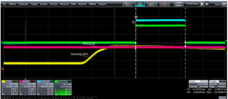
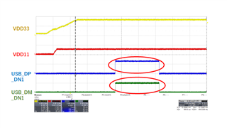
In the following post, I told you that the voltage of USB_DP_DN1 rises due to the influence of BATEN.
There were cases where this pulse width became wider.
Why is the pulse width wider?
Best Regards
Nishie
Part Number: TUSB4020BI
Hi,
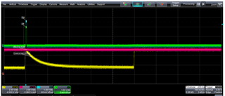
In the following post, I told you that the voltage of USB_DP_DN1 rises due to the influence of BATEN.
There were cases where this pulse width became wider.
Why is the pulse width wider?
Best Regards
Nishie