This thread has been locked.

If you have a related question, please click the "Ask a related question" button in the top right corner. The newly created question will be automatically linked to this question.

DS90UB934-Q1: Serializer ID automatically load failed issue

Part Number: DS90UB934-Q1
Other Parts Discussed in Thread: USB2ANY

Hi Team,

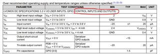
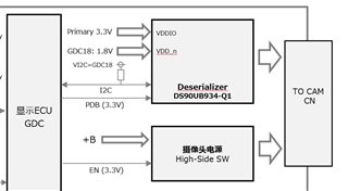
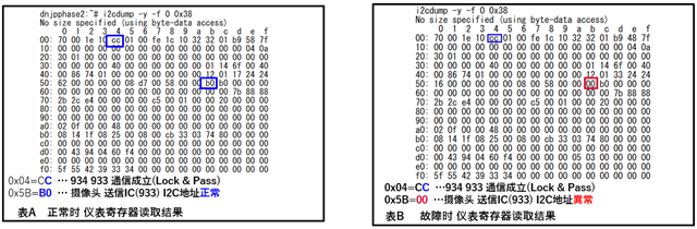
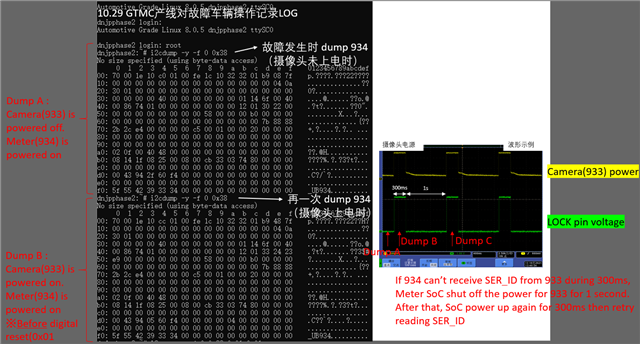
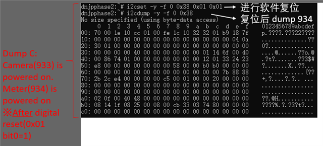
My customer found 933/934 I2C communication failure in production. While LOCK/PASS is ok. 933 address is 0xB0.

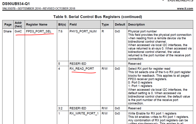
When read 0x5B(SER_ID) in abnormal 934, it returned 0x00. In normal device, SER_ID is 0xB0. Here we want to double confirm this SER_ID fundamental with you:

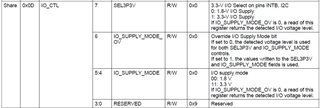
1. How does 933 load SER_ID to 934 during start up?

2. Is there sequencing(or others) requirement of the 933/934 system to let the SER_ID loading successfully?

3. If loading failed(SER_ID=0x00), will it cause the I2C communication failure?

4. Can customer write SER_ID by manual to link the 933?

Can you please help comment at your earliest convenience since it is an urgent case in my customer and Car OEM.

Many thanks.

BR,

Rory

  • Hello Rory,

    Can you please share the values in registers 0x04 and 0x4D of the 934 device?

    1. The SER ID is loaded automatically. 

    2. No, there is no sequencing required, but if you see bit 0x5B[0] "FREEZE DEVICE ID," you will see that that setting this bit prevents the auto-loading of the SER device ID from the forward channel.

    3. If loading fails, it would mean that there is no link and so you will not be able to communicate with 933. 

    4. Yes, you can write to register 0x5B SER_ID, but you need to make sure that you have established link lock with the 933

    Best Regards,

    Shruti More

  • Hello Shruti,

    Please check below registers:

    Normal device: reg0x04:0xCC, reg0x4d: 0x17

    Abnormal device: reg0x04:0xCC, reg0x4d: 0x33

    And below questions need you further confirm:

    1. Is 933 PDB Vih level should refer to CONTROL INPUT or other spec?

    2. In 933 datasheet, we required that V(VDD_n) to PDB VIH delay should be 0 to 16ms, please check below scope shot of the power up sequencing of current 933, is there any risk of this time frame considering the high/low temperature like PDB turns high prior to the VDD_n turns high? I also attached the schematic of 933 below.

    3. Any suggestion to investigate the root cause based on above info?

    BR,

    Rory

  • Hello Rory,

    Have you tried setting register 0x4C to enable the RX port that you are using on the 934?

    After doing so, please check if you are seeing the expected value in registers 0x5B.

    1. Yes, PDB is considered to be an input (control) to the SER.

    2. PDB should be brought high after all power supplies on the board have stabilized. It looks like it's reaching the VIH min value before VDD_n turns high. Which signal is being probed for VDD_n exactly? (VDDT/VDDPLL/VDDCML/VDDD?)

    Best Regards,

    Shruti 

  • Hello Shruti,

    For the 934 register question, customer set the 0x4C=01h. It means that the RX_READ PORT="0" and RX_WRITE_PORT_0= "1"

    I think it is correct setting.

    Thanks,

    Yuta Kurimoto

  • Hi Shruti,

    If PDB logic Vih is refer to input control, the minimum Vih is 2V, so Vih timing is M8 in the scope shot, 90% V(VDD_n) timing is M7, there is 7.9286ms(t3 value in the d/s) delay measured in the scope shot. Can you please help check again?

    And now we suspect that if the device and external capacitor temperature variation may cause t3 shorter. How about your thought?

    I will ask for the detail probed VDD_n signal, is there any difference between these four signal?

    For the LOCK status change and BCC CRC error in 0x4d, any finding or test we can do to investigate?

    Thanks.

    Rory

  • Hello Yuta and Rory,

    Thanks for sharing the 0x4C register value.

    How frequently are you experiencing the issue of not being able to read the SER_ID from the 934? What are the power up sequence details? Are you powering up the 933 SER first and then the 934 DES? Or is it some other situation?

    Can you try doing a digital reset (register 0x01) of the DES (934) after link up with the SER (933)?

    I looked again at the picture and saw that the blue PDB signal is less than 2V in the white circled region and becomes high after 9.8064s (as seen in pic). This power up sequencing looks fine. 

    I am also looking into your other questions and will get back to you in a few days. 

    Best Regards,

    Shruti 

  • Hello Shruti,

    >How frequently are you experiencing the issue of not being able to read the SER_ID from the 934? What are the power up sequence details? Are you >powering up the 933 SER first and then the 934 DES? Or is it some other situation?

    A. From SOP to now, we know about 12pcs in near 9Kpcs. It seems that no clear pattern has been found, but once it reappears, the anomaly will always exist. Camera in Sunny side, we do the repeated test, no recurrence. One thing notice, all camera in our product line, we do high and low temperature start-up test. But we don't know if there are some tests in Meter(Denso-934) side.

    >Can you try doing a digital reset (register 0x01) of the DES (934) after link up with the SER (933)?

    A. Customer will try it soon

    Customer really want to know the root cause why 934 load the SER_ID=00 during LOCK=H. Car OEM rushing Tier1 and TI to find out the root cause so I need below answer as soon as possible.

    Q. Customer want to enter test mode(Device enter test mode when GPO2=High during PDB=High) intentionally in order to check if the LOCK status will High and check if SER_ID will become 00 in the test mode. Can you please let me know how much pull-up voltage, value of pull-up resistance and the time when start pull high the GPO2 pin?

    Q. Can you let me know the detail condition of test mode?

    - Will the LOCK status become HIGH in the test mode?

    - Can they access local I2C of 933 and 934?

    - Can they use back channel and forward channel in test mode?

    - Will the video signal be forwarded to SoC via 934?

    - Will the 934 load SER_ID from 933?

    Thanks,

    Yuta Kurimoto

  • Hi Shruti,

    We found that in 934 side, VDDIO=3.3V, VI2C=1.8V, PDB pull up to 3.3V. Now they did not over write 0x0D register, reg 0x0D=B9. Do you think there will be the root cause of BC communication failure?

    And to solve this VI2C voltage level configuration, need we set IO_SUPPLY_MODE_OV or IO_SUPPLY_MODE or either of them?

    I also searched below e2e post, it said This voltage is applied to I2C and PDB pins together, since PDB(3.3V) and VI2C(1.8V) from different level, is it necessary to make them same?

    https://e2e.ti.com/support/interface-group/interface/f/interface-forum/992198/ds90ub954-q1-i2c-with-1-8v-and-vddio-3-3v

    BR

    Rory

  • Hello Yuta,

    At power up the GPIO are disabled and by default include a 25-kΩ (typical) pulldown resistor and have VDDIO logic levels. Register GPIO_INPUT_CTL (0x0F) sets the GPIO as an input or output. In register GPIO_PD_CTL (0xBE), in the 934, you will see that you can disable/enable GPIO2 pull down resistor. Because the GPIOs have this 25-kΩ resistor, an external resistor is not needed. Register GPIO2_PIN_CTL (0x12) controls what the gpio outputs. Please see register 0x12 in the 934 datasheet. It can be configured to show the lock status of the RX port(s). 

    I assume you are referring to the built-in-self-test. Please refer to section "7.5.2.4.1 BIST Configuration and Status," in the 934 datasheet. You will see that "While the lock indications are required to identify the beginning of proper data reception, for any link failures or data corruption, the best indication is the contents of the error counter in the BIST_ERR_COUNT register 0x57 for each RX port." 

    The link lock is checked during BIST. During BIST, the serializer outputs a continuous stream of a pseudo-random sequence and the deserializer detects the test pattern and monitors it for errors; this stream of a pseudo-random sequence is not forwarded to the SoC. Also, during the actual BIST process, the des (934) will not receive the SER ID since the normal data pattern is replaced with the BIST pattern. 

    There is also a training video on BIST (built-in-self-test): https://training.ti.com/diagnostics-status-monitoring-data-protection-and-built-self-test-bist?context=1134310-1139222-1134312 

    Hello Rory,

    I am not sure if that is the root cause, I will have to look into that. By default, both I2C and I/O are tied to VDDIO. So, you will need to program the 0x0D register setting to override what you actually want to use. PDB and I2C don't have to be the same. 

    Best Regards,

    Shruti

  • Hi Shruti,

    Please help double confirm it.

    And further questions need you kind help:

    1. Is that ok to only write 0x0D bit6=1 then 0x0D bit7=0 or any other config need to be done?

    2. If VI2C=1.8V, VCCIO=3.3V, no 0x0D over write, VIH of VI2C(min) if 0.7VCCIO=2.31V, is there any risk to send over write command since high level(1.8V) is less than 2.31V. Or must customer to tie VCCIO and VI2C together in hardware?

    3. Confirm if the root cause is from the VI2C setting, and the detail explanation.

    Many thanks.

    BR,

    Rory

  • Hello Shruti,

    Thanks for your answers. In addition to the Rory’s question, let me ask some question.

    Q1. During BIST mode, is there any possibility to be LOCK STS=1?

    Q2. During BIST mode, can we access local I2C of 934?

    Q3. If the above answers are YES, how long will it take to finish the BIST for initialize? I assume customer will see SER ID=00 if they can read the local register during BIST.

    Thanks,

    Yuta Kurimoto

  • Hello Rory,

    You can write to register 0x0D to configure both bits 6 and 7 at the same time. 

    However, we recommend that you use the default voltage levels for PDB and I2C. Please follow the typical connection diagram in the datasheet which shows how the supply voltage pins are connected.

    The issue you are having is not being able to read the SER_ID (reg 0x5B). Are you able to read all other registers in the 934? If you are, then power supply voltage of PDB and I2C should not be an issue. I think you should check if there is no lock loss. For any link failures or data corruption, you can monitor the lock and indicate whether you have a valid link, the best indication is the contents of the error counter in the de-serializer, or the BIST error counter register.

    "One of the most important things you should do is check the lock status. This lock output it's through a pin, or you can also read back. But typically, you'll connect the lock output pin directly to the GPIO on the processor. This really serves a purpose to validate that there is link integrity between the serializer and de-serializer. When the lock goes high, that means the phase lock loop in the de-serializer is validating the data, and the clock recovered from the serial input is available.

    If the lock status is low, then the PLL's not locked the incoming data. So you can't really trust that things are going to be transferred correctly from the serialized to the de-serializer.

    This lock pin status, you should also use that for gating the I2C communication. A lot of times, during initialization, when you are changing the frequency, say, of an imager, or the processor output frequency is still stabilizing, you may have some issues where it's trying to lock onto the signal, or relocking during that initial startup phase. So during that condition where you don't have a lock, the command sent. There won't be an ACK. And the I2C command may not be received properly. So you always want to make sure you check for a lock signal before you attempt any I2C command, especially over the remote slaves."

    Hello Yuta,

    Yes, the Lock status register will always indicate if you have lock or not. 

    Yes, when BIST is running on the 934, you can access the local registers of 934 via I2C. 

    There is no set time for how long will it take to finish the BIST. You can find an example BIST code in the training video (link in previous reply). Yes SER_ID will not get updated since the des (934) will not receive the SER ID as the normal data pattern is replaced with the BIST pattern. 

    You can learn more details about BIST in sections 2.4, 3.1 and 3.2 in this app note: https://www.ti.com/lit/an/snla267a/snla267a.pdf?ts=1635203798738&ref_url=https%253A%252F%252Fwww.ti.com%252Fproduct%252FDS90UB953-Q1 

    Best Regards,

    Shruti 

  • Hello Shruti,

    Attached is the 934 register dump. Left one is normal one(They can read SER_ID). Right one is abnormal(Can't read SER_ID)

    They can read all other local register of 934, so supply voltage of PDB and I2C should not be an issue as you mentioned.

    In both cases, the LOCK, PASS status are High. And the 0x57(BIST_ERR_COUNT) is 00.

    Do you have your thought about the root cause by checking these register dump?

    Thanks,

    Yuta Kurimoto

  • Hello Shruti,

    Now customer change the 0x0D  to 0x79, but Back channel cannot connect successfully. Must them to tie VI2C and VDDIO at the same voltage on hardware or is it ok to over-write 0x0D in register? Do you have met similar case before?

    In below e2e link,  said the I2C and PDB must be together.

    https://e2e.ti.com/support/interface-group/interface/f/interface-forum/992198/ds90ub954-q1-i2c-with-1-8v-and-vddio-3-3v/3664641?tisearch=e2e-sitesearch&keymatch=IO_CTL#3664641

    And for the LOCK, PASS status, it is stable, we also test the MAP, the link margin is ok.

    BR,

    Rory

  • Hello Shruti,

    Sorry for asking again.

    Do you come up with any root cause from 933 side why SER_ID become 00? we need to list up all of possible root cause from both 933 and 934 side.

    This is external E2E forum so I will send you the 933 side circuit diagram and power up sequence by email.

    Thanks,

    Yuta Kurimoto

  • Hello Yuta and Rory,

    We recommend that the supply voltage of PDB/IO and I2C should be the same. I have not met a similar case before where they are different. Please try supplying the same voltage to I/O and I2C (VDDIO pin).

    Can you please try doing a digital reset (register 0x01) of the DES (934) after link up with the SER (933)?

    Best Regards,

    Shruti

  • Hi Shruti,

    Currently in customer side, it is hard for them to tie I/O and I2C voltage together. Since we asked them to change the 0x0D [7:6] but did not work. So they ask that must 934 work on same I/O and I2C voltage level, or is it ok to keep them different and change the 0x0D?

    For the second item, they tried the digital reset but the issue did not disappear either.

    We have no additional idea and been pressed from customer, can you please help check further action we can do to solve this problem? Any thing we can do please let us know. Thanks.

    BR,

    Rory

  • Hello Rory,

    We recommend using the same voltage level for the I/O and I2C. In your case, it may work if you set reg 0x0D. 

    Thank you for being patient. I am putting together a failure analysis PowerPoint. Please give me 1-2 days. 

    Also, can you please clarify information about the power up sequence and share more information about the testing being done at two different places (Sunny and Denso)? It seems like there are two tests being done and for one of them there is no issue, but for the other one there is an issue

    Do you power up the 933 first, then 934. wait for x amount of time, then PDB 934 with the 933 still powered up? Can you please clarify?

    It will also be helpful if you could send me the register dump of the 933 as well. 

    You can also check if the back channel is fully functional or not. In the information you shared via email, it says that there is NACK when the SoC tries to send I2C command to the 933 via the back channel.

    Best Regards,

    Shruti

  • Hello Shruti,

    Thanks for your strong support! 

    For the failure analysis report, I believe you heard the background from Heather or Chanakya. Right?

    Once you finished creating the failure analysis(FTA) power point, can you please send to me and Rory? I think we had better move to internal E2E or email.

    >>Also, can you please clarify information about the power up sequence and share more information about the testing being done at two different places

    >>(Sunny and Denso)? It seems like there are two tests being done and for one of them there is no issue, but for the other one there is an issue

    The presentation material is all information which I have now. If needed, I will ask more detail test condition for them.

    >>Do you power up the 933 first, then 934. wait for x amount of time, then PDB 934 with the 933 still powered up? Can you please clarify?

    The 934 is powered up firstly. After that the external High side switch turns on then 933 is powered up secondary.

    >>It will also be helpful if you could send me the register dump of the 933 as well. 

    They don't have the information now but I requested them to get 933 register dump by using USB2ANY. This is because their camera doesn't have MCU on the board, and 934 can't send back channel so they need to read 933 local register via USB2ANY.

    Regards,

    Yuta Kurimoto

  • Hello Yuta,

    Thank you for your answers. I am almost done with the slides and will email them to you. 

    We recommend that you power up the SER first and then the DES. 

    Best Regards,

    Shruti

  • Hello Shruti,

    Thanks, I'm looking for your email.

    It is first time for me to hear that we recommend to power up SER first and then DES. Is there any datasheet or application note which describe it? If they power up DES first, what is the concern?

    In the meantime, customer trying Digital reset(0x01 bit0=1) solution to solve this issue. After the digital reset, the SER_ID can be read. It seems this digital reset solution working well but I want to double check if there is any other conflict about digital reset solution? (For example, in case only resetting 934 side, is there anything to take care such as retry timing, register value, etc.?)

    Thanks,

    Yuta Kurimoto

  • Hello Yuta,

    Powering up the SER first is not a hard requirement. However, we recommend it as a best practice to reset the DES after the SERs have powered up to allow for more consistent lock times & AEQ settings.

    You are doing a digital reset bit 0 which resets the entire digital block except the registers. So, I don't think you need to worry about resetting any registers.

    Thanks for your patience, I will send you the email soon.

    Best Regards,

    Shruti

  • Hello Shruti,

    Now customer care about that if every digital reset can solve this BC communication issue with high confidence so that they can use this as walk around solution currently. Thanks.

    BR,

    Rory

  • Hello Rory,

    We recommend doing a digital reset after PDB or after SER initially locks since the SER is powering up second, after the DES is already powered up. If this "SER_ID not loading," issue is resolving with the digital reset work around, then you should be able to use it. 

    Best Regards,

    Shruti

  • Hello Shruti,

    Can you please share the Failure analysis material ASAP?

    Customer Is rushing us to provide material everyday. We need to report it to the all of stakeholder including OEM director so I need material ASAP.

    Thanks,

    Yuta Kurimoto

  • Hello Yuta,

    I emailed you the slides. 

    Best,

    Shruti

  • Hello Shruti,

    I sent the "FTA results" and "Timing chart" by email. And I write current request to you again.

    If you can't answer these soon, I would appreciate if you can let me know the estimated answer date.

    - FTA

    Q. For the FTA results, can you please let me know what is the next step? If there is something to investigate more, please let me know.

    Q. In customer's reproduction test, they found the issue is easily reproduced at -30C. I think it may be a hint to reach the root cause. Can you let me know your thought about this? Now I'm requesting customer to get result of Margin analysis at -30C.

    - Timing chart

    Q. When is the SER_ID load timing?(Before LOCK? or After LOCK?). If possible, can you disclose the detail of flow chart inside 933 and 934? it will be very helpful.

    TI field team is having daily customer meeting with Tier1 and OEM everyday from 3 weeks ago. Customer pushes us to provide each answer as soon as possible. I really want to solve this soon. Your help is essential for this.

    Thanks,

    Yuta Kurimoto

  • Hello Yuta,

    Yes, I got your email; thank you for sharing. Please allow me a few days to think about other possibilities for this issue. 

    I believe Denso should look into checking item number 8 again for the test conditions at which they see the issue. Since the SER_ID is not loading at -30C, they should do a margin analysis for that test condition, like you pointed out. 

    There is no material about the SER_ID load timing that I can share with you currently. However, I am looking into finding more information about it.

    I greatly appreciate your patience. 

    Best Regards,

    Shruti

  • Hello Shruti,

    Thanks for your update.

    Can you please let me know the estimated answer date for(Nov/??) for each items? Without the date information, customer can't make a plan for future action.

    Regards,

    Yuta Kurimoto

  • Hello Yuta,

    Please allow a few days as we discussed in our meeting today. Thank you.

    Best Regards,

    Shruti

  • Hello Shruti,

    Thanks for your support.

    As I mention in today's meeting, we need your answer about FTA, Timing chart by this Friday(Santa clara time).

    Currently customer is performing margin analysis at -30C, and summarizing test set up. Once I get update from them, I'll let you know.

    Thanks,

    Yuta Kurimoto

  • Hello Yuta,

    Thank you. Yes, I am working on it. 

    Best Regards,

    Shruti

  • Hello Shruti,

    Thanks for your strong support.

    As we talked, I'm looking for the FTA, Timing chart answers by this Friday Santa clara time.

    My expectation is to get the answer by ppt file. Once you share the file, I'll send it to customer on Saturday Japan time.

    For the margin analysis at -30C, customer is still struggling. Because the USB2ANY is 3.3V pull up, and their 934 is 1.8V pull-up. So they are creating level shift circuit.

    Regards,

    Yuta Kurimoto 

  • Hello,

    I sent you the email yesterday.

    Best Regards,

    Shruti

  • Yuta, Shruti,

    Have there been any updates on this thread? What exactly is needed to close this issue?

    Best Regards,

    Casey

  • Hello Casey,

    I have a question about SER_ID(0x5B bit7:1) register in 934. After LOCK is stable and 934 loaded SER_ID from 933, If SoC overwrite the SER_ID register as different value, is the SER_ID maintained? 

    (For example, the 934 firstly load 0x58 value as SER_ID from 933 during LOCK is stable. After that SoC overwrite the 934's 0x5B=0x00. In this case, is the SER_ID in 0x5B register maintained as 0x00? or Will the 934 immediately re-load the correct SER_ID(0x5B=0x58) from 933 because forward channel frame which contains SER_ID is send every 3.7us?)

    I'm seeking if there any possible root cause outside IC.

    Regards,

    Yuta Kurimoto

  • Hello Yuta,

    You can write the SER_ID in the DES at start up since you know the default value (in 933) and then communicate with the 933.

    The default SER_ID is 0xB0 in the 933. I am not sure why you care saying "correct SER_ID(0x5B=0x58)."

    I am not sure why you would want to write 0x00 to reg 0x5B while the SER_ID in 933 is 0xB0. Can you please explain how that would help to check root cause outside IC?

    Thanks,

    Best Regards,

    Shruti

  • Hello Shruti,

    I made mistake. The correct SER_ID is 0x5B=0xB0.

    I understand SoC of 934 side don't need to write 0x5B because SER_ID is auto-loaded from 933. However I'm suspecting if SoC of 934 side had made some mistake to write the 0x5B (for example, incorrect program sequence, incorrect SDA/SCL high low timing, mistake for Read/Write command)

    That is the reason why I want to ask if the 0x5B register. If FREEZE DEVICE ID=1, it prevents auto loading so the 0x5B can't reload SER_ID. If FREEZE DEVICE ID=0, will the 0x5B reload 0xB0 as soon as it receive forward channel frame?

    Thanks,

    Yuta Kurimoto

  • Hello Yuta,

    0x5B[0] "FREEZE DEVICE ID," this bit prevents the auto-loading of the SER device ID from the forward channel. So, yes, if they enable this bit, then the SER_ID won't be loaded when it is received from the forward channel. 

    So, yes, If FREEZE DEVICE ID=0, the 0x5B register loads 0xB0 as soon as it is received via the forward channel frame. 

    Can they share their programming sequence and how they are reading and writing to the 934 registers at start-up? Are they running any script like imager initialization script on the 934 at start up?

    Best Regards,

    Shruti

  • Hello Shruti,

    I sent the programming sequence on Nov/16 but I will re-send by email.

    Thanks,

    Yuta Kurimoto

  • Hello Yuta,

    I found your email. Thanks. 

    Best,

    Shruti