This thread has been locked.

If you have a related question, please click the "Ask a related question" button in the top right corner. The newly created question will be automatically linked to this question.

HD3SS214: HD3SS214:

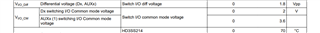
Part Number: HD3SS214

Hello,

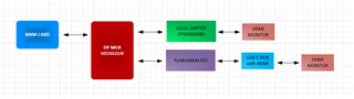
I would like to correct my schematic. Please refer to the design picture below. The bottom part works via USB type C and the top part doesn't work. This is because I have AC coupling caps on AUX N/P lanes between the MXM card and H2/H1 AUXp/AUXn pins of HD3SS214I and PTN3360DBS needs DC coupling . If I replace the AC coupling caps with 0 ohms, the top circuit works but bottom won't work as TUSB1046AI-DCI needs AC coupling. 

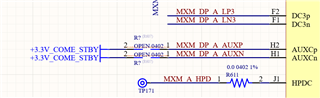
On the AUX P/N lines, is it okay to DC couple between MXM card and HD3SS214I and AC couple between HD3SS214I and TUSB1046AI-DCI? So the entire path from MXM card to HDMI via the level translator is DC coupled while through the USB C circuit is AC coupled. 


  • Hi,

    Yes, you can do that. This way the MXM card to the TUSB1046 is still AC coupled, and the MXM card to the PTN3360 is DC coupled.  

    Thanks

    David

  • Thanks,

    I wasn't sure if it allowed to DC couple from MXM to HD3SS214I and AC couple from HD3SS214I to TUSB1046. Can I send you the schematic?

  • Hi,

    I do not see an issue with the schematic.

    Thanks

    David 

  • Thank you.

    So for my understanding:

    Internally, HD3SS214I  doesn't depend on any DC bias from the source side or the destination side? For example, if I AC couple on both sides it should still work with the USB C circuit? Just curious if either the left or right path needs DC bias. 

    Right now my top path has no AC coupling. Bottom path has AC coupling from MUX to USB C circuit but not from MXM to MUX.

  • Hi,

    The HD3SS214 still requires a bias voltage as shown below. If you place the capacitors on one side of the switch, then the bias voltage needs to be provided by the other side of the switch. If you place the capacitors on both sides of the switch, then an external biasing voltage should be provided.

    Bottom path has AC coupling from MUX to USB C circuit but not from MXM to MUX -> So the biasing voltage comes from the MXM and you need to make sure the biasing voltage from the MXM meets the HD3SS214 common mode voltage requirement shown above.

    My top path has no AC coupling -> Either side of the HD3SS214 gets biased, you still need to make sure the biasing voltage meets the HD3SS214 common mode voltage requirement shown above.

    Thanks

    David 

  • Well,

    right now the top path worked when I made the AC caps 0V in my current board. Only change I am making to my new design, not sent to you yet, is I am changing the DP-to-HDMI level shifter to Diodes INC PI3HDX511DZLEX. I don't see a common mode voltage in it nor on the MXM card. I would think an MXM card is designed to a spec correct? What do I exactly ask as I have a contact I can ask the right question

    The bottom path worked fine with the AC caps to the left side of the MUX. Now I am shifting it to the right side. So logically, since the top circuit worked with BIAS obtained from the MXM card when I did a test it should technically work now correct?

    Should I place some open pads to provide external biasing if needed? How do I do it?

  • Hi,

    right now the top path worked when I made the AC caps 0V in my current board. Only change I am making to my new design, not sent to you yet, is I am changing the DP-to-HDMI level shifter to Diodes INC PI3HDX511DZLEX. I don't see a common mode voltage in it nor on the MXM card. I would think an MXM card is designed to a spec correct? What do I exactly ask as I have a contact I can ask the right question

    ***  The AUX common mode voltage should be set by the I2C pullup to 3.3V (R613 and R617).

    The bottom path worked fine with the AC caps to the left side of the MUX. Now I am shifting it to the right side. So logically, since the top circuit worked with BIAS obtained from the MXM card when I did a test it should technically work now correct?

    *** With the cap on the left side of the MUX, the MUX AUX common mode voltage is set by the pullup and pulldown resistor on the AUX bus. Now with the cap moved to the right side of the MUX, the MUX common mode voltage is set by the MXM. You need to double check with the MXM vendor to make sure the MXM AUX common mode voltage is within the MUX AUX common mode voltage range of 0 to 3.6V.

    Should I place some open pads to provide external biasing if needed? How do I do it?

    *** You need to AC couple both sides of the HD3SS214, and then have 100k pullup resistor to the biasing voltage 

    Thanks

    David 

  • Understood.

    Good suggestion. I provided a mechanism as shown below in case I AC couple both sides. I have asked the MXM vendor. In general can I make an assumption that it should work for any graphics card because they are all industry standard? In case they don't come back with an answer.

  • Hi,

    Can you send me the full schematic? If the GPU is DP spec compliant, then I would assume the GPU AUX common mode voltage to be between 0 and 2V, which is within the HD3SS214 spec.

    Thanks

    David

  • I sent you privately. Yes the GPU is an MXM card which is DP compliant. Because we have used it before via the DP-HDMI mux to HDMI connector and it worked.

  • Hi,

    With the GPU being DP compliant, I do not see an issue with the current schematic.

    Thanks
    David