


Part Number: XIO2001
Hi Support Team.
Please tell me the following information of XIO2001IZAJ.
・Copper pad diameter(mm)
・Copper pad thickness(mm)
・Solder mask openting diameter(mm)
・Solder mask openting thickness(mm)
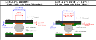
↓Reference diagram
Thanks,
Part Number: XIO2001
Hi Support Team.
Please tell me the following information of XIO2001IZAJ.
・Copper pad diameter(mm)
・Copper pad thickness(mm)
・Solder mask openting diameter(mm)
・Solder mask openting thickness(mm)
↓Reference diagram
Thanks,

