This thread has been locked.

If you have a related question, please click the "Ask a related question" button in the top right corner. The newly created question will be automatically linked to this question.

SN65DSI85: Optimization of 0x28 CHA_SYNC_DELAY_LOW setting

Part Number: SN65DSI85

Hello,

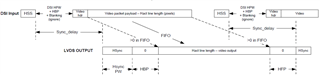
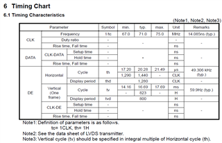
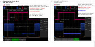
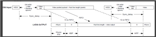
Our customer is facing 0xE5 "80" CHA_SYNCH_ERR, after debugging they found 0x28 CHA_SYNC_DELAY_LOW value is key parameter.

The datasheet described like "The Sync delay must be programmed to at least 32 pixel clocks to ensure proper operation."

However if use "21Hex, 33Dec" Sync error is occurred then change it to less than "1Dhex,Dec29" resulted in 0xE5 CHA_SYNCH_ERR is disappeared.

How can we find the optimized number of 0x28 CHA_SYNC_DELAY_LOW setting? DSI tuner is not mentioned this setting.


Regards,

Mochizuki

  • Mochizuki-san

    The LVDS output rate must be less than or equal to the DSI input rate. The first line of a video frame shall start with a VSS packet, and all other lines start with VSE or HSS. The position of the synchronization packets in time is of utmost importance since this has a direct impact on the visual performance of the display panel; that is, these packets generate the HS and VS (horizontal and vertical sync) signals on the LVDS interface after the delay programmed into CHA_SYNC_DELAY_LOW/HIGH (CSR 0x28.7:0 and 0x29.3:0). So it sounds like the LVDS output rate does not match with the DSI input rate and you have to use the CHA_SYNC_DELAY_LOW to compensate for the difference.

    Thanks

    David

  • Hello David,

    Thank you for your support.


    Our customer's configuration is DSI CLK 222MHz from i.MX8M, LVDS output is 74MHz. 0x0B REFCLK_MULTIPLIER setting is "02h" Divide by 3.

    Also H Blanking time registers setting were

    0x2c HSYNC_PULSE_WIDTH "32h" 50clk

    0x34 H_BACK_PORCH  "32h" 50clk

    0x38 H_FRONT_PORCH "3Ch" 60clk

    So, total H Blanking time is 160clk

    With 0x28 CHA_SYNC_DELAY "21h" 33clk, we were facing 0xE5 SYNC_ERROR "80h" CHA_SYNCH_ERR


    They had tried another experiment which is modified ratio inside of H Blanking time as below.

    0x2c HSYNC_PULSE_WIDTH "8Ch" 140clk 

    0x34 H_BACK_PORCH "0Ah" 10clk

    0x38 H_FRONT_PORCH "0Ah" 10clk

    Total H Blanking time is keeping 160clk, not changed.

    Then resulted in 0xE5 SYNC_ERROR is disappeared even 0x28 CHA_SYNC_DELAY is "21h" 33clk.


    Which countermeasure is right way to fix CHA_SYNCH_ERR flag? Optimize value of CHA_SYNC_DELAY or HSYNC_PULSE_WIDTH?

    Still we could not get error detection mechanism or threshold value of CHA_SYNCH_ERR flag rise up.

    Is that matter of HSYNC_PULSE position between some of internal reference clock?

    What is negative impact if we use 20h 32clk or less clk for 0x28 CHA_SYNC_DELAY?


    Regards,

    Mochizuki

  • Mochizuki-san

    Have you checked the link time on the DSI input and the LVDS output? There is no need to match horizontal or vertical video CSR configurations to the DSI input values except for the CH*_ACTIVE_LINE_LENGTH (number of active pixel). In other words, as long as the line time is met, the blanking parameters on the LVDS side do not need to exactly match the blanking parameters on the DSI side. However, the active pixels always need to match.

    Thanks

    David

  • Hi David,

    I have ran DSI tuner using the customer's parameters.

    Please find attached .dsi files.(Changed .dsi to .txt)


    %CHIP3%PVCATexas%PMCAtexmex%RPCA1280%RLCA800%PVCB%PMCB%RPCB%RLCB%LVCM0%HPWA50%HBPA50%HFPA60%HACA1280%HTOA1440%HPWB%HBPB%HFPB%HACB%HTOB0%VPWA3%VBPA10%VFPA10%VACA823%VTOA846%VPWB%VBPB%VFPB%VACB%VTOB0%PCKN74%LCKS0%RCKM%MULT0%DCKA222%DIVI2%LCKR74.0%FMTA1%DEPA1%HSPA0%VSPA0%BPPA1%FMTB1%DEPB0%HSPB1%VSPB1%BPPB0%PRDA1280x800%PRDBx%DSCM0%LREO1%LRCE1%LPCA0%BMCA0%SMCA0%LPCB0%BMCB0%SMCB0%DHPA50%DHBA50%DHFA60%DHAA1280%DHTA1440%DHPB%DHBB%DHFB%DHAB%DHTB%DVPA3%DVBA10%DVFA10%DVAA823%DVTA846%DVPB%DVBB%DVFB%DVAB%DVTB%DDRA222%NOLA3%VIMA2%LCRP%DDRB%NOLB0%VIMB0%RCRP
    %CHIP3%PVCATexas%PMCAtexmex%RPCA1280%RLCA800%PVCB%PMCB%RPCB%RLCB%LVCM0%HPWA140%HBPA10%HFPA10%HACA1280%HTOA1440%HPWB%HBPB%HFPB%HACB%HTOB0%VPWA3%VBPA10%VFPA10%VACA823%VTOA846%VPWB%VBPB%VFPB%VACB%VTOB0%PCKN74%LCKS0%RCKM%MULT0%DCKA222%DIVI2%LCKR74.0%FMTA1%DEPA1%HSPA0%VSPA0%BPPA1%FMTB1%DEPB0%HSPB1%VSPB1%BPPB0%PRDA1280x800%PRDBx%DSCM0%LREO1%LRCE1%LPCA0%BMCA0%SMCA0%LPCB0%BMCB0%SMCB0%DHPA50%DHBA50%DHFA60%DHAA1280%DHTA1440%DHPB%DHBB%DHFB%DHAB%DHTB%DVPA3%DVBA10%DVFA10%DVAA823%DVTA846%DVPB%DVBB%DVFB%DVAB%DVTB%DDRA222%NOLA3%VIMA2%LCRP%DDRB%NOLB0%VIMB0%RCRP

    0xE5 error.dsi : We were seeing 0xE5 SYNC_ERROR "80h" CHA_SYNCH_ERR with 0x28 CHA_SYNC_DELAY "21h" 33clk on ES board.

    0x2c HSYNC_PULSE_WIDTH "32h" 50clk

    0x34 H_BACK_PORCH "32h" 50clk

    0x38 H_FRONT_PORCH "3Ch" 60clk


    No error.dsi : 0xE5 SYNC_ERROR is disappeared with 0x28 CHA_SYNC_DELAY "21h" 33clk on ES board.

    0x2c HSYNC_PULSE_WIDTH "32h" 140clk

    0x34 H_BACK_PORCH "32h" 10clk

    0x38 H_FRONT_PORCH "3Ch" 10clk


    However "Outputs" panel showed both are same number, it looks not duplicate actual ES board error function.

    Would you suggest us optimized parameters using this DSI input and LVDS output interface configuration. 

    Regards,

    Mochizuki

  • No error.xls0xE5 error.xls

    Please change it from .xls to .dsi

  • Mochizuki-san

    The CHA_SYNC_DELAY, as stated in the datasheet this field controls the delay in pixel clocks from when an HSync or VSync is received on the DSI to when it is transmitted on the LVDS interface.

    You can use this formula to calculate the sync_delay

    sync_delay > ( ( (DSI_HPW + DSI_HBP) * LVDS_Mpix/s / DSI_Mpix/s ) - (LVDS_Hsync_PW + LVDS_HBP)

    DSI_Mpix/s = DSI_CLK * 2* number of lane / BPP

    Between the no_error and 0xE5_error case, you are keeping the LVDS_HSYNC_PW and LVDS_HBP the same value, but changing the DSI_HPW and DSI_HBP value, so the sync_delay value needs to be updated as well.

    Thanks

    David

  • Hi David,

    Thank you for your suggestion. We applied your calculation to find minimum CHA_SYNC_DELAY.


    <Case1> Same as .dsi file

    CHA_SYNC_DELAY: At 33dec, SYNC ERROR on 0x80.  At 5dec to 29dec No SYNC ERROR on the board.

    DSI   HPW:50 / HBP:50 / HFP:60

    LVDS  HPW:50 / HBP:50 / HFP:60


    CHA_SYNC_DELAY > ((50+50)* 74 / 74) (50+50) = 100 100 = 0 

    In this calculation result showed CHA_SYNC_DELAY > 0

    However in our experiment, An error is still occurred between 0 to 4dec and more than 29 for CHA_SYNC_DELAY setting.

    Is there another parameter to calculate optimized CHA_SYNC_DELAY value?


    <Case2> Here is another example, different from .dsi file

    CHA_SYNC_DELAY: at 33dec, No SYNC ERROR on 0x80 on the board.

    DSI HPW:140 / HBP:10 / HFP:10

    LVDS HPW:140 / HBP:10 / HFP:10


    CHA_SYNC_DELAY > ((10+140)* 74 / 74) (10+140) = 150 150 = 0

    It is same calculation result with pervious case. But No SYNC ERROR on 0x80 when CHA_SYNC_DELAY is 33dec

    Why we can see multiple behavior of error detection function on the board with same calculation result settings?


    Regards,

    Mochizuki

  • Mochizuki-san

    The sync delay must be programmed to at least 32 pixel clocks to ensure proper operation. This accounts for the DSI85 internal synchronization time. On top of the 32 pixel clocks, you need to add more, if needed, using the formula in my previous response.

    Thanks
    David 

  • Hi David,

    Thank you for your prompt reply.

    Under this situation, case2 setting looks better because it is good match both of board verification result and the device requirement calculation formula. Our customer will take this parameters for production unit.


    The other hand, we are still having curiosity, why case1 setting show us strange sync error even it meet all requirements?

    Could you point out what is concern of case1 parameter setting?


    Regards,

    Mochizuki

  • Mochizuki-san

    For case 1, can they measure the end of HSS on the DSI input to the start of HSYNC on the LVDS side. Does 32 pixel clock delay also produce the SYNC_ERROR?

    Thanks

    David

  • Hello David,

    Our customer captured six waveforms as attached.

    The setting condition and expected error flag are below.


    H Blanking HFP:60 / HPW:50 / HBP:50

    #1 SYNC DELAY : 21(HEX)/33(DEC) SYNC ERROR (0xE5:80) --> Over 32, should not be Error.

    #2 SYNC DELAY : 06(HEX)/06(DEC) No ERROR (0xE5:00) --> Below 32, should be Error.

    #3 SYNC DELAY : FF (HEX)/255(DEC) SYNC ERROR (0xE5:80) --> Over 32, should not be Error.


    H Blanking setting   HFP:10 / HPW:140 / HBP:10

    #4 SYNC DELAY : 21(HEX)/33(DEC) No ERROR (0xE5:00) --> Aligned with the description

    #5 SYNC DELAY : 06(HEX)/06(DEC) No ERROR (0xE5:00)   --> Below 32, should be Error.

    #6 SYNC DELAY : 8F(HEX)/143(DEC) SYNC ERROR (0xE5:80) -- Over 32, should not be Error.


    Would you tell us your findings what is discrepancy between SYNC DELAY requirement on the datasheet and those waveform.

    SN65DSI85 Sync Delay.pdf

    Regards,

    Mochizuki

  • Mochizuki-san

    The SYNC_DELAY is when an HSync or VSync is received on the DSI to when it is transmitted on the LVDS interface. Can they re-measure the SYNC_DELAY between the end of HSS on the DSI to the beginning of HSS on the LVDS side? 

    What is the Hactive line length value?

    Thanks

    David 

  • Hi David,

    In our captured waveforms, you can see actual SYNC DELAY time on Right side waveform in the pdf file which attached yesterday's message. Have you found our pdf file?

    eg. #1. capture. SYNC DELAY setting is 33dec, on Right side waveform there is 0.0135us x 33 = 0.4455us delay. It is perfectly matched with register setting.

    And the Hactive line length value is 1280 as in DSI tuner parameter which we had previously attached.


    Here is our questions would you please give us your suggestions to move forward.

    Q1: Isn't this your requested capture of "the SYNC_DELAY between the end of HSS on the DSI to the beginning of HSS on the LVDS side" ? Or something else?

    Q2: Then what can you find from this waveform? There is an error 0xE5:80, even we meet "more than 32dec" SYNC DELAY requirement.

    How can we fix this error flag?

    Q3: On the datasheet recommendation SYNC DELAY should be more than 33dec, but acctulay we can see an error at 128dec and not have an error at 6dec.

    What is involved another parameter to rise 0xE5:80 flag?


    Regards,

    Mochizuki

  • Mochozuki-san

    Please below block diagram for the SYNC_DELAY definition.

    The SYNC_DELAY is defined as the delay between the end of HSS on the DSI interface to the beginning of HSYNC on the LVDS interface.

    So when you change the HFP from 10 to 50, I think you created a line time mismatch between the DSI and LVDS which will cause CHA_SYNC_ERR.

    Thanks

    David

  • Hi David,

    Could you specifically tell us the line time mismatch area in the timing chart in attached files.

    It seems HFP setting would be key parameter to avoid SYNC ERR, could you tell us setting guideline.

    Is it possible to get the suggestions from design team?


    Regards,

    Mochizuki

    SN65DSI85_SYNC DELAY.pptx

  • Mochizuki-san

    Please give me couple days and let me have an internal discussion.

    Thanks
    David

  • Mochizuki-san

    Please see this e2e FAQ guide, item #4, https://e2e.ti.com/support/interface-group/interface/f/interface-forum/852871/faq-sn65dsi84-no-display-output-with-sn65dsi83-sn65dsi84-sn65dsi85.

    Can they measure the line time on both the DSI and the LVDS interface and see if the line time is the same with the two different blanking parameters? 

    Also, does the LVDS panel support both blanking parameters?

    Thanks

    David

  • Hi David,

    Thank you for introducing the training material.

    We had gone through the materials.

    Actually we had been confirming DSI tuner output tab result, it was no concern. And in our captuerd waveform both of Branking time were same value .

    There is not How to optimize Sync Delay value in those materials. Sorry to say but we could not get new information.


    Regards,

    Mochizuki

  • Mochizuki-san

    Can the LVDS panel support both blanking parameters?

    Thanks

    David 

  • Hi David,

    That is correct LCD panel support 1440 and 823 as below.

    Anyway we expected interface condition between LVDS output and LCD panel will not cause of Sync Error from the device, but we can see failed image on the panel.


    Regards,

    Mochizuki

  • Mochizuki-san

    I am trying to understand the two captured scope waveforms. On the failing waveform, what is the pulse that I have circled in red?

    Thanks

    David 

  • Hello David,

    That is a packet from DSI.

    We can see this packet at earlier position when H Blanking setting is HFP:10 / HPW:140 / HBP:10.

    Regards,

    Mochizuki

  • Mochizuki-san

    If you look at the timing diagram I shared earlier, the SYNC delay is defined as the end of HSS on the DSI input and the beginning of HSYNC on the LVDS output. For the case of HFP 60, I wonder if the circled pulse is the HSYNC from the DSI source.

    Thanks

    David

  • Hi David,

    It looks DSI processor behavior would be concern of 0xE5:80 error with HFP:50 in that case.

    So far we could not see the formula of 0xE5:80 error flag generation timing boundary condition of HFP setting aligned with real device function.

    I understand it will be difficult to create and verify after several years later from the device is released to market.

    Lastly our customer wants to get your comment for their No error configuration that is HFP:10 / HPW:140 / HBP:10 / SYNC DELAY: 21(HEX)/33(DEC)”.  Is this still have concern or acceptable setting?

    Regards,

    Mochizuki

  • Mochizuki-san

    So far from their measurement and testing I do not see an issue with this setting.

    Thanks
    David

  • Hello David,

    Our customer has another project with 15inch LCD panel.

    For the combination with various LCD panel characteristics, we want to confirm most simple parameter setting procedure as below.


    1. 0x28 CHA_SYNC_DELAY would be 33(Dec) fix value, no need to try another number.

    2. Run DSI tuner and enter LCD panel characteristics to find out total "H blanking". Then breakdown it to HPW, HBP and HFP value as you like.

    3. If 0xE5:80 Sync Error is not appeared, this configuration would be suitable.


    So, without to know a formula of Sync Delay value boundary condition and acceptable area of HFP value, we think this procedure is good enough. To close our customer's concern we would like to have your acceptance once again.


    Regards,

    Mochizuki

  • Mochizuki-san

    Please see this training video, https://training.ti.com/configuring-sn65dsi8x-single-channel-dsi-single-link-lvds-operation.

    The Horizontal blanking is divided among HPW, HBP, and HFP. Otherwise your procedure is correct.

    Thanks

    David