Part Number: DS90UB953-Q1
OV2778 to GW5400(ISP) ICC Register Setting We have questions that have questions.
# Camera info
- 1920 x 1080 @ 30fps
- XVCLK : 24Mhz
- Linear 12 bit RAW, 10 bit Raw
- MIPI 4 Lane
- RGB-IR Sensor
1) DS90UB953, None synchronous mode Register Setting Data
2) DS90UB954, Des Register Setting Data
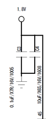
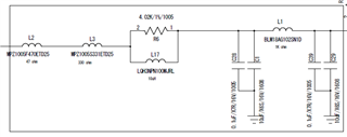
In addition, the attachment is 953, 954 circuit diagrams. Please refer to Please review it.
1) LG_FORD_RGBIR_OV2778_MAX20446_R5.4_211005_ICC.pdf
2) 211016_FORD_TI954_Testboard_R0.pdf
In addition, the following is a setting that was mainly used as Sync Mode in our waste.
You can also partially modify it.
- DS90UB954
[REGPAGE_954_Des]
DEVADR = 0x60 /
REGW = X01, X06 / // Reset
REGW = X02, X1E / // General Config
REGW = X0C, X81 / // ENABLE RX PORT 0
#REGW = X18, X00 / // Frame CTL
#REGW = X1F, X00 / // CSI_data_spd_1600
REGW = X1F, X02 / // CSI_data_spd_800 (Default)
REGW = X21, X01 / // FWD_CTL2 //04
REGW = X4C, X01 / // FPD3_PORT_SEL
REGW = X6D, X7C / // PORT_CONFIG //7C
#REGW = X7C, X00 / // PORT_CONFIG2
REGW = X58, X5E / // BCC_CONFIG (I2C CONT)
REGW = X5C, X30 / // Ser Addr
REGW = X5D, X6C / // Sensor Addr
REGW = X65, X6C / // Sensor Addr
REGW = X33, X01 / // CSI CTL (MIPI4LANE) // 01
REGW = X20, X20 / // Enable Port 0
#REGW = X4A, X10 / // KP _TEST
- DS90UB953
[REGPAGE_953_SER]
DEVADR = 0x30 /
REGW = X0D, X80 /
REGW = X0E, X80 /
#REGW = X02, X72 /
LG_FORD_RGBIR_OV2778_MAX20446_R5.4_211005_ICC.pdf211016_FORD_TI954_Testboard_R0.pdf