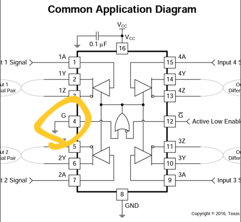
Hi team,
I had a customer that wants to design in AM26C31 and had some questions.
About the reference design as the datasheet, why pin G needs to connect to GND? It can't meet the true table.

This thread has been locked.
If you have a related question, please click the "Ask a related question" button in the top right corner. The newly created question will be automatically linked to this question.
Hi team,
I had a customer that wants to design in AM26C31 and had some questions.
About the reference design as the datasheet, why pin G needs to connect to GND? It can't meet the true table.

Hi Len,
The table shows that the device has high-impedance outputs only when G is low and G̅ is high. In the example you provided, tying G low allows the user to use G̅ as a negative-logic input (active low enable). Another implementation would be to tie G̅ high. This would allow G to be used as an positive-logic input (active high enable).
The first figure you included is just a common/typical application. It is not the only way to implement the G/G̅ enables.
Keep in mind that, although "X" in the Function Table indicates that the state of the input is irrelevant, it is ill-advised to leave an unused input pin floating on a device. This is why the image you referenced shows the unused input tied to GND.
Best,
Danny