This thread has been locked.

If you have a related question, please click the "Ask a related question" button in the top right corner. The newly created question will be automatically linked to this question.

SN65DP159: Setup & Initial Trimming

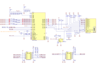
Part Number: SN65DP159

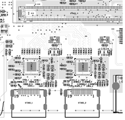
We are using the DP159 in two Designs, connected to an Xilinx FPGA, as a transmitter to a monitor.

The problem is, we have a few monitors working very well and a lot of monitors we can not get to work properly.

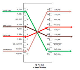
The DP159 has a lot of registers and functionality, but exactly that makes it very hard for us to find a good setup. What we need is some kind of instruction for setup and trimming the chip to work with most of the monitors. If this is not possible, we need an instruction how to configure the monitors individual.

So I can separate my request in two questions:

  1. Is there an optimal setup to get the DP159 working with most of the monitors, and how should the registers be configured, therefore? (maybe some kind of register map with optimal values)
  2. How should we proceed a trimming of the DP159 by testing it with different register values to get an individual monitor to work?
  • Hi,

    Are you configuring the DP159 in I2C or pin-strap mode? 

    Can you share your schematic and layout? And have you run the HDMI1.4/2.0 electrical compliance on this design?

    Thanks

    David

  • Hi David,

    thanks for your answer in advance. Good to see that there is someone who wants to help. I can post the schematic and the top of the layout. I hope this helps.

    There are two similar HDMI interfaces on the board. Therefore you can see them both beneath each other.

    The connector above is a module connector to an FPGA module board.

    What do you mean exactly with "run the HDMI1.4/2.0 electrical compliance". Something like that?
    7BM85_0E.pdf

    The answer would be no, since yet.

  • Let me add one more information, we set the SWAP_EN bit to 1 because we need the lane reversal.
    An we have already exchanged the VADJ Ressistor to 7k.

  • Hi,

    Does the FPGA support the clock stretching as an I2C master on the DDC bus? The DP159 implements the clock stretching. If the FPGA does not support clock stretching, then we need to implement the DP159 DDC snooping.

    The pullup on the SDA_SNK and SCL_SNK needs to be 2k to be HDMI compliant. 

    By "run the HDMI1.4/2.0 electrical compliance", I mean the HDMI electrical compliance test to verify the design signal integrity.

    It looks like you are running the DP159 in I2C mode. The default I2C registers value should able to run HDMI1.4. If you run HDMI1.4 resolution,  can you measure the clock output frequency and see if the frequency is correct?

    I will also point you to this app note which detailed the configuration of DP159 in the I2C mode. www.ti.com/.../slla468.pdf.

    Thanks

    David

  • Hi David,

    we can get the EDID Data from the monitors not workking as well, therefore I would ask if this can be either a problem we should check. We can do some Rework with wires and a levelshifter here, but this is a very offensive action on the electronics.

    We already measured the clock, it is 148.5MHz for a 1080p HDMI. So it seems to be ok. Like I said, there are several Monitors that work very good with the board. And yes we are using the board in I2C mode, sorry for the missing answer here.

    Can you check the link you added again please, I can not get there. I get the answer:

    "It looks like we’ve encountered some resistance.

    (Sorry, the page you’re looking for can’t be found.)"

  • Hi,

    Here is the link to the app note, https://www.ti.com/lit/an/slla468/slla468.pdf

    I am looking at the schematic again, is lane 0 and lane 1 being connected correctly? 

    If the clock lane looks correct, can you also look at one of the data lanes?

    Thanks

    David

  • Hi David,

    your last tip was really good! We checked the Reversal again and you are right. The Clock Lane and the Data Lane 1 are correct with the reversal. But Data Lane 0 and Data Lane 2 have to be switched. We did this with some wires on the board and now the other Monitor is working as well.

    The wired thing was, that some Monitors could work with that some will not. Therefore I think we searched so long for the problem.

    We will try to find a solution in the FPGA maybe, but this is not your topic.

    Thanks for your help!