Part Number: DS90UB948-Q1
Hi team,
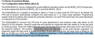
I'd like to ask if we can modify the order of the LVDS pins through registers? As I can see in the datasheet, LVDS channels D0 to D3 carry ODD pixel data, and LVDS channels D4 to D7 carry EVEN pixel data, could it be modified?