This thread has been locked.

If you have a related question, please click the "Ask a related question" button in the top right corner. The newly created question will be automatically linked to this question.

PCF8574

Other Parts Discussed in Thread: PCF8574, MSP430F2252


Dear guys, 


I am trying to make a wind vane using 8 photo interrupters, since I have used I2C ports of microcontroller for other sensor therefore I am using PCF8574 (I2C expander) that will communication with MSP430F2252. 

The Idea is to  I am trying to read one byte value from the slave. Could you please tell me how I can do this?


How can I interpret in use my idea. Thanks. 


Any help would be appreciateable. 
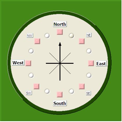
 

North is bit1

North & NE is bit 2

NE is bit 3

NE & East bit 4 and goes on to the end. 


I found this code in C example but  

//

//                                MSP430F22x4

//                              -----------------

//                  /|\ /|\ /|\|              XIN|-

//                  10k 10k  | |                 |

//       PCF8574     |   |   --|RST          XOUT|-

//       ---------   |   |     |                 |

//  --->|P0    SDA|<-|---+---->|P3.1/UCB0SDA     |

//  --->|P1       |  |         |                 |

//  --->|P2       |  |         |                 |

//  --->|P3    SCL|<-+---------|P3.2/UCB0SCL     |

//  <---|P4       |            |                 |

//  <---|P5       |            |                 |

//  <---|P6       |            |                 |

//  <---|P7       |            |                 |

//   +--|A0,A1,A2 |            |                 |

//   |  |         |            |                 |

//  \|/

//

//  Andreas Dannenberg

//  Texas Instruments Inc.

//  March 2006

//  Built with CCE Version: 3.2.0 and IAR Embedded Workbench Version: 3.41A

//******************************************************************************

#include "msp430x22x4.h"


void main(void)

{

  WDTCTL = WDTPW + WDTHOLD;                 // Stop Watchdog Timer

  P3SEL |= 0x06;                            // Assign I2C pins to USCI_B0

  UCB0CTL1 |= UCSWRST;                      // Enable SW reset

  UCB0CTL0 = UCMST+UCMODE_3+UCSYNC;         // I2C Master, synchronous mode

  UCB0CTL1 = UCSSEL_2+UCSWRST;              // Use SMCLK, keep SW reset

  UCB0BR0 = 12;                             // fSCL = SMCLK/12 = ~100kHz

  UCB0BR1 = 0;

  UCB0I2CSA = 0x20;                         // Set slave address

  UCB0CTL1 &= ~UCSWRST;                     // Clear SW reset, resume operation

  IE2 |= UCB0RXIE;                          // Enable RX interrupt

  TACCTL0 = CCIE;                           // TACCR0 interrupt enabled

  TACTL = TASSEL_2 + MC_2;                  // SMCLK, contmode


  while (1)

  {

    __bis_SR_register(CPUOFF + GIE);        // CPU off, interrupts enabled

    UCB0CTL1 &= ~UCTR;                      // I2C RX

    UCB0CTL1 |= UCTXSTT;                    // I2C start condition

    while (UCB0CTL1 & UCTXSTT);             // Loop until I2C STT is sent

    UCB0CTL1 |= UCTR + UCTXSTT;             // I2C TX, start condition

    __bis_SR_register(CPUOFF + GIE);        // CPU off, interrupts enabled

    while (UCB0CTL1 & UCTXSTT);             // Loop until I2C STT is sent

    UCB0CTL1 |= UCTXSTP;                    // I2C stop condition after 1st TX

  }

}


#pragma vector = TIMERA0_VECTOR

__interrupt void TA0_ISR(void)

{

  __bic_SR_register_on_exit(CPUOFF);        // Exit LPM0

}


// USCI_B0 Data ISR

#pragma vector = USCIAB0TX_VECTOR

__interrupt void USCIAB0TX_ISR(void)

{

  UCB0TXBUF = (UCB0RXBUF << 4) | 0x0f;      // Move RX data to TX

  __bic_SR_register_on_exit(CPUOFF);        // Exit LPM0

}


  • Here is a link to the datasheet for the PCF8574: http://focus.ti.com/lit/ds/symlink/pcf8574.pdf

    I am not an expert on MSP430 programming, so I cannot comment on the code. I am, however, familiar with the PCF8574.

    I assume you are familiar with I2C protocol, but if not, pages 7-10 of the datasheet should have the information you need.

    Upon power-up of the PCF8574, all of the I/Os are in the INPUT state, where each pin has a 100uA current source pulling to Vcc. I will assume your photo-interrupters are configured to produce a logic high or low value on these I/Os. I will also assume that the one or two photo-interrupters activated by the wind direction will produce a logic low value.

    If you are only reading the I/O states, you will only need to perform I2C reads from the device.

    The I2C address for reading the device is [0] [1] [0] [0] [A2] [A1] [A0] [1]. Assuming the three address pins are connected to VSS, the address byte is 01000001 or 21h.

    To read a byte, the MSP430 provides the I2C START sequence, followed by the address byte, then the Acknowledge (Ack). After that, the eight data bits will reflect the states on the I/Os. The data sequence is P7, P6, P5, P4, P3, P2, P1, P0 so if, as you state, P1 represents North, and that is the indicated direction, then the data byte will be 11111101.

    After the data byte, you can provide an ACK (SDA=0) to immediately read another byte, or you can keep SDA=1 to end the transaction, requiring the entire sequence to read another byte.

    Please reply if you need further information.

    Regards,

    Ken Williams - Texas Instruments


  • Dear Ken, 

    Thanks for writing such a long forum for me. I do have an idea how I2C works. I would just like to ask you few questions and if you can answer them this would probably resolve my issue. 

    Your all assumptions are indeed correct. Photo-interrupters are configured to produce logic High (5V) and logic low (0V). At one time it will be either one or two photo-interrupters will be at high state and rest will be at low state.  

    I have used I2C communication for some sensors, for which I had to setup tramission (including slave address), transmit address ( could be a control address) and then setup receive ( again including slave address) and then read the sensor address.


    All I was just confused about the slave address, what it should be? Then should I follow the same procedure I used for reading sensor or just setup receive (including slave address as you mentioned above 0x21h, if A0, A1, A2 pins are connected to VSS) and read the slave, which I assumed give me one byte reading?

    Thats it for now. Thanks again.

    Regards, 

    Mo. 


  • Muhammed,

    Is seems like the previous I2C devices you used required a command byte (sub-address) which had to be input before performing a read. The PCF8574 only has one register for write and read, so you only need to transmit the slave address with the R/W bit set high. Then, after the address is ack'd, the next byte on SDA will be the read data from the 8 inputs.

    With all address pins tied to 0, the transaction will look like this:

    ST | 0 | 0 | 1 | 0 | 0 | 0 | 0 | 1 | Ack | P7 | P6 | P5 | P4 | P3 | P2 | P1 | P0 | Ack | P7 | P6 | P5 | P4 | P3 | P2 | P1 | P0 | Ack | ...

    Repeat the last nine cycles for as many bytes as you want to read.

    On the first Ack, the PCF8574 pulls SDA low. On the second, and all others, the Master device pulls SDA low. If the master does not pull SDA low, the PCF8574 will end the transmission and require the whole sequence again. 

    Please reply if you need further information.

    Regards,

    Ken Williams

    Texas Instruments